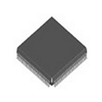
BCM5208KPF Broadcom, BCM5208KPF Datasheet - Page 16

BCM5208KPF
Manufacturer Part Number
BCM5208KPF
Description
Manufacturer
Broadcom
Datasheet
1.BCM5208KPF.pdf
(62 pages)
Specifications of BCM5208KPF
Number Of Receivers
4
Data Rate
10/100Mbps
Operating Temperature Classification
Commercial
Operating Supply Voltage (min)
3.14V
Mounting
Surface Mount
Operating Temperature (max)
70C
Operating Temperature (min)
0C
Lead Free Status / RoHS Status
Not Compliant
Available stocks
Company
Part Number
Manufacturer
Quantity
Price
Company:
Part Number:
BCM5208KPF
Manufacturer:
ON
Quantity:
201
Company:
Part Number:
BCM5208KPF
Manufacturer:
BCM
Quantity:
846
Part Number:
BCM5208KPF
Manufacturer:
BROADCOM
Quantity:
20 000
n BCM5208
Page 8
PIN
32, 207,
156, 125
17, 190,
172, 140
19, 20, 21,
23
192, 193,
194, 195
170, 169
168, 167
136, 134
24,196,
166, 133
18, 191,
171, 139
26, 206,
157, 131
25, 205,
151, 132
118
117
119
MODE
38, 39, 40
Note: # = active low, I = digital input, O = digital output, I/O = bidirectional, I
digital input w/ internal pull-up, I
I/O
by {Port #}.
138, 137
PD
= bidirectional w/ internal pull-down, B = Bias. Bus Naming Convention: pin label followed by [MSB:LSB] followed
PIN LABEL
TXER {1:4}
RXC {1:4}
RXD[3:0] {1}
RXD[3:0] {2}
RXD[3:0] {3}
RXD[3:0] {4}
RXDV {1:4}
RXER {1:4}
CRS {1:4}
COL/RXEN
{1:4}
MDIO
MDC
RESET#
PHYAD [4:2]
PD
TYPE
I
O
O
O
O
O
I/O
I/O
I
I
I
PD
PD
PU
PD
3S
3S
3S
3S
3S
= digital input w/ internal pull-down, O
PD
PD
Table 4: Pin Descriptions(Continued)
DESCRIPTION
Transmit Error. Active high. Asserting TXER when TXEN is asserted causes
transmission of 100BASE-X’s designated “bad code” in lieu of normal 4B5B
encoded data on the wires. No action is taken in 10BASE-T mode if TXER is
asserted. If not used, may be left open or pulled to ground.
Receive Clock. 25 MHz output in 100BASE-X mode and 2.5 MHz output in
10BASE-T mode. This clock is recovered from the incoming data on the cable
inputs. Becomes 10 MHz when RPTR=SER10=1. In DTE applications, RXC is a
continuously running output clock resynchronized at the start of each incoming
packet. This synchronization may result in an elongated period during one cycle
when RXDV is low.
Receive Data Outputs. Nibble-wide receive data is driven out these pins
synchronously to RXC. RXD[3] is the most significant bit.
Receive Data Valid. Active high. Indicates that a receive frame is in progress,
and that the data stream present on the RXD output pins is valid.
Receive Error Detected. Active high. Indicates that there has been an error
during a receive frame.
Carrier Sense. Active high. Indicates traffic on link. In 100BASE-X modes, CRS
is asserted when a non-idle condition is detected in the receive data stream and
deasserted when idle or a valid end of stream delimiter is detected. In 10BASE-
T mode, CRS is asserted when a valid preamble is detected and deasserted
when end-of-file or an idle condition is detected. In DTE mode, CRS is also
asserted during transmission of packets. CRS is an asynchronous output signal.
Collision Detect. In half-duplex DTE modes, active high output indicates that a
collision has occurred. In full-duplex mode, COL remains low. COL is an
asynchronous output signal.
Receive Enable. In Repeater mode, RXEN is an active high input. Enables
BCM5208 to drive MII bus. MII outputs are forced high-Z when RXEN is low.
Management Data I/O. This serial input/output bit is used to read from and write
to the MII registers. The data value on the MDIO pin is valid and latched on the
rising edge of MDC.
Management Data Clock. The MDC clock input must be provided to allow MII
management functions. Clock frequencies up to 12.5 MHz are supported.
Reset. Active Low. Resets the BCM5208. Pin not included in NAND chain.
PHY Address Selects. These inputs set the three MSB’s for the MII
management PHY addresses. The two LSB’s, PHYAD [1:0], are internally wired
to each of the four ports: PHYAD [00] = Port 1,..., PHYAD [11] = Port 4. Also
serve as test control inputs along with TESTEN and NANDMD[1:0] to select the
NAND-chain test mode.
B r o a d c o m C o r p o r a t i o n
OD
= open-drain output, O
A
= analog input, O
Document 5208-DS03-R¥¥¥¥¥
A
= analog output, I
3S
= three-state output,
November 3, 1999
PU
=


