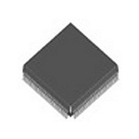
BCM5208KPF Broadcom, BCM5208KPF Datasheet - Page 18

BCM5208KPF
Manufacturer Part Number
BCM5208KPF
Description
Manufacturer
Broadcom
Datasheet
1.BCM5208KPF.pdf
(62 pages)
Specifications of BCM5208KPF
Number Of Receivers
4
Data Rate
10/100Mbps
Operating Temperature Classification
Commercial
Operating Supply Voltage (min)
3.14V
Mounting
Surface Mount
Operating Temperature (max)
70C
Operating Temperature (min)
0C
Lead Free Status / RoHS Status
Not Compliant
Available stocks
Company
Part Number
Manufacturer
Quantity
Price
Company:
Part Number:
BCM5208KPF
Manufacturer:
ON
Quantity:
201
Company:
Part Number:
BCM5208KPF
Manufacturer:
BCM
Quantity:
846
Part Number:
BCM5208KPF
Manufacturer:
BROADCOM
Quantity:
20 000
n BCM5208
Page 10
PIN
204, 185,
177, 158
202, 183,
179, 160
201, 182,
180, 161
JTAG
99
100
101
102
103
44
POWER
181
7
8
77
80
59, 63, 72,
76, 81, 85,
94, 98
Note: # = active low, I = digital input, O = digital output, I/O = bidirectional, I
digital input w/ internal pull-up, I
I/O
by {Port #}.
PD
= bidirectional w/ internal pull-down, B = Bias. Bus Naming Convention: pin label followed by [MSB:LSB] followed
PIN LABEL
SP100LED#
{1:4}
XMTLED# {1:4}
INTR# {1:4}
FDXLED# {1:4}
Ser SDO# {2}
RCVLED# {1:4}
ACTLED# {1:4}
Ser SCLK# {2}
TDI
TDO
TMS
TCK
TRST#
DLLTEST
IVDD
PLLVDD
PLLGND
BIASVDD
BIASGND
AVDD
PD
TYPE
O
O
O
I
O
I
I
I
I
PU
PU
PU
PU
PU
OD
OD
3S
= digital input w/ internal pull-down, O
Table 4: Pin Descriptions(Continued)
DESCRIPTION
Speed 100 LED. Driven low when operating in 100BASE-X modes and high
when operating in 10BASE-T modes.
Transmit Activity LED. Active low output. The transmit activity LED is driven
low for approximately 80ms each time there is transmit activity while in the link
pass state. When INTR mode is enabled, the pin becomes an interrupt output.
When FDX LED mode is enabled, the pin becomes FDXLED output. When the
Serial LED mode is enabled, pin 183 becomes the Serial LED mode data output
signal.
Receive Activity LED. Active low output. The receive activity LED is driven low
for approximately 80ms each time there is receive activity while in the link pass
state. When in either INTR or FDXLED modes, this pin becomes ACTLED output
for either receive or transmit activity. When the Serial LED mode is enabled, pin
182 becomes the Serial LED mode clock signal.
Test Data Input. Serial data input to the JTAG TAP Controller. Sampled on the
rising edge of TCK. If unused, may be left unconnected.
Test Data Output. Serial data output from the JTAG TAP Controller. Updated on
the falling edge of TCK. Actively driven both high and low when enabled; high
impedance otherwise.
Test Mode Select. Single control input to the JTAG TAP Controller used to
traverse the test-logic state machine. Sampled on the rising edge of TCK. If
unused, may be left unconnected.
Test Clock. Clock input used to synchronize JTAG control and data transfers. If
unused, may be left unconnected.
Test Reset. Asynchronous active-low reset input to the JTAG TAP Controller.
Must be held low during power-up to insure the TAP Controller initializes to the
test-logic-reset state. May be pulled low continuously when JTAG functions are
not used.
DLT Bypass Test Enable. This pin is for factory test only, and must be
connected to DVDD or left floating.
Input VDD. +5.0 V or +3.3V. If any of the inputs are driven to 5.0V, this pin must
be connected to the 5.0V supply. If none of the inputs are driven above 3.3V, this
pin may be connected to the 3.3V supply.
Phase Locked Loop VDD
Phase Locked Loop GND
Bias VDD
Bias GND
Analog VDD
B r o a d c o m C o r p o r a t i o n
OD
= open-drain output, O
A
= analog input, O
Document 5208-DS03-R¥¥¥¥¥
A
= analog output, I
3S
= three-state output,
November 3, 1999
PU
=


