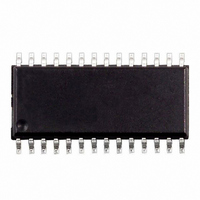
M41ST87WMX6 STMicroelectronics, M41ST87WMX6 Datasheet - Page 17

M41ST87WMX6
Manufacturer Part Number
M41ST87WMX6
Description
IC SUPERVISOR RTC 160X8 28-SOIC
Manufacturer
STMicroelectronics
Type
Clock/Calendar/Supervisorr
Specifications of M41ST87WMX6
Memory Size
160B
Time Format
HH:MM:SS:hh (24 hr)
Date Format
YY-MM-DD-dd
Interface
I²C, 2-Wire Serial
Voltage - Supply
2.7 V ~ 3.6 V
Operating Temperature
-40°C ~ 85°C
Mounting Type
Surface Mount
Package / Case
28-SOIC, 28-SOH (8.48mm Width)
Function
Clock/Calendar/Alarm/Timer Interrupt
Rtc Memory Size
160 Byte
Supply Voltage (max)
3.6 V
Supply Voltage (min)
2.7 V
Maximum Operating Temperature
+ 85 C
Minimum Operating Temperature
- 40 C
Mounting Style
SMD/SMT
Rtc Bus Interface
Serial (2-Wire, I2C)
Lead Free Status / RoHS Status
Lead free / RoHS Compliant
Other names
497-5370-5
M41ST87WMX6
M41ST87WMX6
Available stocks
Company
Part Number
Manufacturer
Quantity
Price
Part Number:
M41ST87WMX6
Manufacturer:
ST
Quantity:
20 000
Company:
Part Number:
M41ST87WMX6TR
Manufacturer:
MBI
Quantity:
12 000
M41ST87Y, M41ST87W
2.3
Figure 12. WRITE mode sequence
Figure 13. WRITE cycle timing: RTC & external SRAM control signals
1. Available in SOX28 (MX) package only.
2.4
BUS ACTIVITY:
MASTER
SDA LINE
BUS ACTIVITY:
EX
E CON
WRITE mode
In this mode the master transmitter transmits to the M41ST87Y/W slave receiver. Bus
protocol is shown in
(R/W = 0) is placed on the bus and indicates to the addressed device that word address An
will follow and is to be written to the on-chip address pointer. The data word to be written to
the memory is strobed in next and the internal address pointer is incremented to the next
memory location within the RAM on the reception of an acknowledge clock. The
M41ST87Y/W slave receiver will send an acknowledge clock to the master transmitter after
it has received the slave address (see
the word address and each data byte.
Data retention mode
With valid V
or WRITE cycles. Should the supply voltage decay, the M41ST87Y/W will automatically
deselect, write protecting itself (and any external SRAM) when V
(max) and V
accomplished by internally inhibiting access to the clock registers. At this time, the reset pin
(RST) is driven active and will remain active until V
RAM access is inhibited in a similar manner by forcing E
within 0.2 volts of the V
of-tolerance condition. When V
(1)
(1)
S
ADDRESS
CC
PFD
SLAVE
applied, the M41ST87Y/W can be accessed as described above with READ
(min) (see
t
EXPD
Figure
BAT
ADDRESS (An)
. E
12. Following the START condition and slave address, a logic '0'
Figure 28 on page
WORD
CON
Doc ID 9497 Rev 9
CC
will remain at this level as long as V
falls below the battery backup switchover voltage (V
Figure 9 on page
DATA n
t
EXPD
46,
Table 19 on page
CC
returns to nominal levels. External
DATA n+1
16) and again after it has received
CON
to a high level. This level is
CC
falls between V
46). This is
CC
DATA n+X
remains at an out-
Operating modes
AI00591
AI03663
PFD
P
SO
17/54
),


