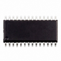
M41ST87WMX6 STMicroelectronics, M41ST87WMX6 Datasheet - Page 18

M41ST87WMX6
Manufacturer Part Number
M41ST87WMX6
Description
IC SUPERVISOR RTC 160X8 28-SOIC
Manufacturer
STMicroelectronics
Type
Clock/Calendar/Supervisorr
Specifications of M41ST87WMX6
Memory Size
160B
Time Format
HH:MM:SS:hh (24 hr)
Date Format
YY-MM-DD-dd
Interface
I²C, 2-Wire Serial
Voltage - Supply
2.7 V ~ 3.6 V
Operating Temperature
-40°C ~ 85°C
Mounting Type
Surface Mount
Package / Case
28-SOIC, 28-SOH (8.48mm Width)
Function
Clock/Calendar/Alarm/Timer Interrupt
Rtc Memory Size
160 Byte
Supply Voltage (max)
3.6 V
Supply Voltage (min)
2.7 V
Maximum Operating Temperature
+ 85 C
Minimum Operating Temperature
- 40 C
Mounting Style
SMD/SMT
Rtc Bus Interface
Serial (2-Wire, I2C)
Lead Free Status / RoHS Status
Lead free / RoHS Compliant
Other names
497-5370-5
M41ST87WMX6
M41ST87WMX6
Available stocks
Company
Part Number
Manufacturer
Quantity
Price
Part Number:
M41ST87WMX6
Manufacturer:
ST
Quantity:
20 000
Company:
Part Number:
M41ST87WMX6TR
Manufacturer:
MBI
Quantity:
12 000
Operating modes
Note:
2.5
2.6
2.6.1
Note:
18/54
1
2
power input is switched from the V
SRAM are maintained from the attached battery supply.
All signal outputs become high impedance. The V
current to the attached memory with less than 0.3 volts drop under this condition. On power
up, when V
E
Most low power SRAMs on the market today can be used with the M41ST87Y/W RTC
SUPERVISOR. There are, however some criteria which should be used in making the final
choice of an SRAM to use. The SRAM must be designed in a way where the chip enable
input disables all other inputs to the SRAM. This allows inputs to the M41ST87Y/W and
SRAMs to be “Don’t Care” once V
guarantee data retention down to V
sufficient to meet the system needs with the chip enable output propagation delays
included. If the SRAM includes a second chip enable pin (E2), this pin should be tied to
V
If data retention lifetime is a critical parameter for the system, it is important to review the
data retention current specifications for the particular SRAMs being evaluated. Most SRAMs
specify a data retention current at 3.0 volts. Manufacturers generally specify a typical
condition for room temperature along with a worst case condition (generally at elevated
temperatures). The system level requirements will determine the choice of which value to
use. The data retention current value of the SRAMs can then be added to the I
the M41ST87Y/W to determine the total current requirements for data retention. The
available battery capacity for the battery of your choice can then be divided by this current to
determine the amount of data retention available.
For a further more detailed review of lifetime calculations, please see application note
AN1012.
Tamper detection circuit
The M41ST87Y/W provides two independent input pins, the tamper pin 1 input (TP1
tamper pin 2 input (TP2
result in the associated setting of the tamper bits (TB1 and/or TB2, in flag register 0Fh) if the
tamper enable bits (TEB1 and/or TEB2) are enabled, for the respective tamper 1 or tamper
2 channels. The TP1
by either 1) closing a switch to ground or V
that was previously closed to ground or V
the TCM
Tamper register bits (tamper 1 and tamper 2)
Tamper enable bits (TEB1 and TEB2)
When set to a logic '1,' this bit will enable the tamper detection circuit. This bit must be set to
'0' in order to clear the associated tamper bits (TB
TEB
When servicing a tamper interrupt, the TEB
set to 1 to again enable the tamper detect circuits.
OUT
CON
X
.
. The RST signal also remains active during this time (see
should be cleared then set again whenever the tamper detect condition is modified.
X
bits and the TPM
CC
returns to a nominal value, write protection continues for t
IN
pin or TP2
IN
), which can be used to monitor two separate signals which can
X
bits in the tamper register (14h and/or 15h).
Doc ID 9497 Rev 9
IN
CC
CC
CC
pin may be set to indicate a tamper event has occurred
falls below V
pin to the battery, and the clock registers and external
= 2.0 volts. The chip enable access time must be
OUT
OUT
x
bits must be cleared to clear the TB
(normally closed), depending on the state of
(normally open), or by 2) opening a switch
OUT
PFD
X
, in 0Fh).
(min). The SRAM should also
pin is capable of supplying 100µA of
Figure 28 on page
M41ST87Y, M41ST87W
rec
by inhibiting
BAT
x
bits, then
value of
46).
IN
) and


