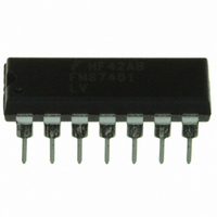
FMS7401LVN14 Fairchild Semiconductor, FMS7401LVN14 Datasheet - Page 21

FMS7401LVN14
Manufacturer Part Number
FMS7401LVN14
Description
IC CTRLR POWER DGTL EEPROM 14DIP
Manufacturer
Fairchild Semiconductor
Datasheet
1.FMS7401LVN.pdf
(81 pages)
Specifications of FMS7401LVN14
Applications
Digital Power Controller
Core Processor
8-Bit
Program Memory Type
EEPROM (1 kB)
Ram Size
64 x 8
Number Of I /o
8
Voltage - Supply
2.7 V ~ 3.6 V
Operating Temperature
-40°C ~ 125°C
Mounting Type
Through Hole
Package / Case
14-DIP (0.300", 7.62mm)
Output Current
5 mA
Input Voltage
2.7 V to 3.6 V
Switching Frequency
2 MHz
Operating Temperature Range
- 40 C to + 125 C
Mounting Style
Through Hole
Lead Free Status / RoHS Status
Lead free / RoHS Compliant
Interface
-
Controller Series
-
Lead Free Status / Rohs Status
Lead free / RoHS Compliant
Other names
FMS7401LVN14_NL
FMS7401LVN14_NL
FMS7401LVN14_NL
Table 7. ADCNTRL2 Register Bit Definitions
4.2
The ADC circuit may be configured to convert analog voltages with a conversion cycle time determined by the ADC clock
(F
section for details. By default, the ADC circuit performs a conversion with every trigger initiated by software setting the
ASTART bit of the ADCNTRL1 register to 1. The ADC circuit may also be configured to perform a conversion automatically
(using the gated auto-sampling mode) with every active (on) edge of the PWM Timer 1 ADSTROBE output signal. Refer to the
following
Before any ADC conversion triggers are issued (by software or automatically) software must configure the voltage reference
(V
ADCNTRL1 register. If using the internal Autozero Amplifier, Uncommitted Amplifier, and Current Source Generator circuits
in the application, software must also configure and enable the desired circuits. Lastly, the F
improve the ADC conversion accuracy.
When performing an ADC conversion where software triggers the conversion, the ASTART bit of the ADCNTRL1 register
remains high (1) symbolizing that a conversion is in progress. The ADC conversion is divided in two phases lasting a total of
13 conversion clock cycles. However, an autozero ADC conversion lasts a total of 20 conversion clock cycles. Refer to the fol-
lowing
cycles, the ADC circuit performs a sample and hold operation to measure fast changing analog signals before converting the
input voltage. The second phase, occupying the last nine cycles, converts the analog input voltage to an 8-bit digital value and
stores it in the ADATA register for easy access by software. Once the converted value is stored in ADATA, the APND bit is trig-
gered and ASTART bit is cleared (symbolizing completion of the conversion cycle). Software cannot rely on the APND bit for
REV. 1.0.3 1/24/05
PRODUCT SPECIFICATION
Bit
REFBY2
COMPSEL
ENAMP
ENDAS
ASPEED[1:0]
ENIS
GAIN
ADCLK
AREF
REFBY2
Bit 7
ADC Conversion Modes
) and analog input channel appropriately. This is done by programming the REFSEL and ACHSEL bits of the
Autozero Amplifier
) and the ASPEED bits of the ADCNTRL2 register. Refer to the following
ADC Gated Auto-sampling Mode
Description
Used to divide the reference clock for the PLL and digital filter of the Programmable Comparator circuit. Refer to the
Circuit
(0) F
(1) F
(0) G4 is connected to the Programmable Comparator’s non-inverting input.
(1) G2 is connected to the Programmable Comparator’s non-inverting input.
(0) Disables the Uncommitted Amplifier (G6 and G7 are normal I/Os).
(1) Enables the Uncommitted Amplifier where G6/-A
amplifier output (A
(0) Enables the Standard ADC Conversion Mode where software must trigger an ADC conversion by setting the ASTART
bit of the ADCNTRL1 register.
(1) Enables the ADC Gated Auto-sampling Mode where PWM Timer 1’s ADSTROBE output to automatically triggers an
ADC conversion.
(0) ADC conversion clock speed = F
(1) ADC conversion clock speed = F
(2) ADC conversion clock speed = F
(3) ADC conversion clock speed = F
(0) Disable Current Source Generator (G3 is a normal I/O).
(1) Enable Current Source Generator where G3/AIN1 sources the I
(0) Disables the Autozero Amplifier (G4 is a normal I/O).
(1) Enables the Autozero Amplifier (with a gain of 16) where G4/AIN0 is its non-inverting input and SR_GND is it inverting
input.
COMPSEL
RCLK2
RCLK2
Bit 6
section of the datasheet for details.
=F
=F
section for details. In the first phase of a standard conversion, occupying the first four conversion
RCLK1
RCLK1
/2
OUT
ENAMP
) is also the ACH5 input to the ADC’s analog mux.
Bit 5
section for details.
ADCNTRL2 Register (addr. 0xA0)
ADCLK
ADCLK
ADCLK
ADCLK
ENDAS
Bit 4
/2
/4
/8
IN
is the inverting input and G7/A
Bit 3
ASPEED[1:0]
SRC
.
ADC Conversion Clock Configuration
Bit 2
ADCLK
OUT
is the amplifier output. The
must be configured to
ENIS
Bit 1
GAIN
FMS7401L
Bit 0
Clock
21


