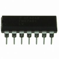
FMS7401LVN14 Fairchild Semiconductor, FMS7401LVN14 Datasheet - Page 47

FMS7401LVN14
Manufacturer Part Number
FMS7401LVN14
Description
IC CTRLR POWER DGTL EEPROM 14DIP
Manufacturer
Fairchild Semiconductor
Datasheet
1.FMS7401LVN.pdf
(81 pages)
Specifications of FMS7401LVN14
Applications
Digital Power Controller
Core Processor
8-Bit
Program Memory Type
EEPROM (1 kB)
Ram Size
64 x 8
Number Of I /o
8
Voltage - Supply
2.7 V ~ 3.6 V
Operating Temperature
-40°C ~ 125°C
Mounting Type
Through Hole
Package / Case
14-DIP (0.300", 7.62mm)
Output Current
5 mA
Input Voltage
2.7 V to 3.6 V
Switching Frequency
2 MHz
Operating Temperature Range
- 40 C to + 125 C
Mounting Style
Through Hole
Lead Free Status / RoHS Status
Lead free / RoHS Compliant
Interface
-
Controller Series
-
Lead Free Status / Rohs Status
Lead free / RoHS Compliant
Other names
FMS7401LVN14_NL
FMS7401LVN14_NL
FMS7401LVN14_NL
FMS7401L
PRODUCT SPECIFICATION
10.1.1 Accumulator (A)
The Accumulator is a general-purpose 8-bit register that is used to hold data and results of arithmetic calculations or data
manipulations.
10.1.2 X-Pointer (X)
The X-Pointer register allows for an 11-bit indexing value to be added to an 8-bit offset creating an effective address used for
reading and writing among the memory space. This provides software with the flexibility of storing lookup tables in the code
1
EEPROM memory space for the core’s accessibility during normal operation.
The microcontroller core allows software to access the entire 11-bit X-Pointer register using the special X-pointer instructions
e.g. LD X, #040H (see
Table
24). Software may also access the register through any of the memory mapped instructions using
the XHI (X[10:8]) and XLO (X[7:0]) variables located at address 0xBE and 0xBF (see
Table
30).
The X register is divided into two sections. The most significant bit (MSB) is write only and selects between the data
(0x000 to 0x0FF) or program (0xC00 to 0xFFF) memory space. The 10 least significant bits (LSBs) represent the specific
address location within the data or program memory space.
For example: If X[10] = 0, the LD A, [#0,X] instruction will take the data at address X[9:0] from the data memory space
(0x000 to 0x0FF) and load it into A. However, if X[10] = 1 the LD A, [#0,X] instruction will take the data at address X[9:0]
from the program memory space (0xC00 to 0xFFF) and load it into A.
The X register can also serve as a counter or temporary storage register. However, this is true only for the 10-LSBs since the
MSB is dedicated for memory space selection.
10.1.3 Program Counter (PC)
The 10-bit Program Counter (PC) register contains the address of the next instruction to be executed. After a system reset,
PC is initialized to 0xC00 and the microcontroller core begins executing the instruction program residing in the code EEPROM
memory at the initialized PC value.
10.1.4 Stack Pointer (SP)
The microcontroller core has an automatic program stack with a 4-bit stack pointer. The stack can be initialized to any location
between addresses 0x30-0x3F in SRAM. Normally, the stack pointer is initialized by one of the first instructions in an applica-
tion program. After a reset, the stack pointer is defaulted to 0xF pointing to the top of the stack at address 0x3F.
The stack is configured as a data structure which decrements from high to low memory. Each time a new address is pushed
onto the stack, the microcontroller core decrements the stack pointer by two. Each time an address is pulled from the stack, the
microcontroller core increments the stack pointer is by two. At any given time, the stack pointer points to the next free location
in the stack.
When a subroutine is called by a jump-to-subroutine (JSR) instruction, the instruction’s address is automatically pushed onto
the stack with the least significant byte first. When the subroutine is finished, a return-from-subroutine (RET) instruction is
executed. The RET instruction pulls the previously stacked return address and loads it into the program counter. Instruction
execution then continues at the pulled return address.
10.1.5 Status Register (SR)
The 8-bit Status Register (SR) contains four condition code indicators (C, H, Z, and N), a global interrupt (G) mask bit, and the
data EEPROM write ready (R) flag. The condition codes are automatically updated by most instructions (see
Table
25). All sta-
tus register bits except for the global interrupt mask are read only when using direct, indirect, or indexed instructions. The carry
and half carry bits may be written by using their special inherent (SC, RC, LDC, RRC and RLC) instructions. Software cannot
restore SR using the traditional microcontroller methods. Refer to the
Interrupt Handling
section for additional details.
47
REV. 1.0.3 1/24/05


