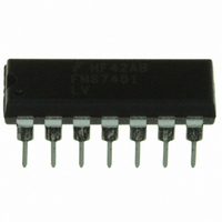
FMS7401LVN14 Fairchild Semiconductor, FMS7401LVN14 Datasheet - Page 29

FMS7401LVN14
Manufacturer Part Number
FMS7401LVN14
Description
IC CTRLR POWER DGTL EEPROM 14DIP
Manufacturer
Fairchild Semiconductor
Datasheet
1.FMS7401LVN.pdf
(81 pages)
Specifications of FMS7401LVN14
Applications
Digital Power Controller
Core Processor
8-Bit
Program Memory Type
EEPROM (1 kB)
Ram Size
64 x 8
Number Of I /o
8
Voltage - Supply
2.7 V ~ 3.6 V
Operating Temperature
-40°C ~ 125°C
Mounting Type
Through Hole
Package / Case
14-DIP (0.300", 7.62mm)
Output Current
5 mA
Input Voltage
2.7 V to 3.6 V
Switching Frequency
2 MHz
Operating Temperature Range
- 40 C to + 125 C
Mounting Style
Through Hole
Lead Free Status / RoHS Status
Lead free / RoHS Compliant
Interface
-
Controller Series
-
Lead Free Status / Rohs Status
Lead free / RoHS Compliant
Other names
FMS7401LVN14_NL
FMS7401LVN14_NL
FMS7401LVN14_NL
Bit 6 of the ADCNTRL2 register is the Programmable Comparator non-inverting input selection (COMPSEL) bit.
COMPSEL=0, the non-inverting input of the Programmable Comparator is the G4/AIN0 device pin. If COMPSEL=1, the non-
inverting input of the Programmable Comparator is the G2/AIN2 device pin. Before enabling the Programmable Comparator
circuit, the selected analog input port pin must be configured as a tri-state input bypassing the I/O circuitry.
Bit 1 of the Comparator Control (COMP) register is the Programmable Comparator circuit’s voltage loop (VLOOP) configura-
tion enable bit. If VLOOP=0, the Programmable Comparator circuit is configured to compare the analog G4/AIN0 or G2/AIN2
input (COMPSEL=0 or 1) to one of the 63 voltage threshold levels. If VLOOP=1, enables the voltage loop configuration where
the analog G4/AIN0 or G2/AIN2 input (COMPSEL=0 or 1) to the Uncommitted (Error) Amplifier output (A
Bit 7 of the Digital Delay (DDELAY) register is the Programmable Comparator circuit enable (COMPEN) bit. If COMPEN=0,
the Programmable Comparator circuit is disabled and the C
circuit is enabled and the C
Bit 0 (COUT) of the Comparator Control (COMP) register is the latched comparator output (C
ble Comparator circuit is enabled, the C
the COMP register. Software may only read the COUT bit to monitor the comparator’s activity. The COUT bit cannot cause
any microcontroller hardware interrupt or any other actions.
REV. 1.0.3 1/24/05
PRODUCT SPECIFICATION
G4/AIN0
G2/AIN2
G7/A
G6/-A
OUT
IN
(ADCNTRL2[6])
COMPSEL
Uncommitted (Error)
OUT
Figure 9. Programmable Comparator Block Diagram (VLOOP = 1)
Amplifier
signal generated by the comparison of the two inputs.
_
+
V
OUT
REF
signal is latched by the main system instruction (F
0.23R
VLOOP
R
OUT
F
signal is low. If COMPEN=1, the Programmable Comparator
RCLK2
EPWM
Comparator
5
+
_
En
DD[3] DD[2] DD[1] DD[0]
3
ACH5
DDELAY
Register
DIGITAL DELAY
COMP Register
Programmable
CIRCUIT
2
Reference
1
ICLK
OUT
0
) clock into the COUT bit of
) signal. If the Programma-
PWMOFF (WKEN[6])
2
OUT
).
C
1
OUT
If
FMS7401L
29


