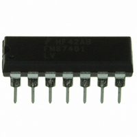
FMS7401LVN14 Fairchild Semiconductor, FMS7401LVN14 Datasheet - Page 54

FMS7401LVN14
Manufacturer Part Number
FMS7401LVN14
Description
IC CTRLR POWER DGTL EEPROM 14DIP
Manufacturer
Fairchild Semiconductor
Datasheet
1.FMS7401LVN.pdf
(81 pages)
Specifications of FMS7401LVN14
Applications
Digital Power Controller
Core Processor
8-Bit
Program Memory Type
EEPROM (1 kB)
Ram Size
64 x 8
Number Of I /o
8
Voltage - Supply
2.7 V ~ 3.6 V
Operating Temperature
-40°C ~ 125°C
Mounting Type
Through Hole
Package / Case
14-DIP (0.300", 7.62mm)
Output Current
5 mA
Input Voltage
2.7 V to 3.6 V
Switching Frequency
2 MHz
Operating Temperature Range
- 40 C to + 125 C
Mounting Style
Through Hole
Lead Free Status / RoHS Status
Lead free / RoHS Compliant
Interface
-
Controller Series
-
Lead Free Status / Rohs Status
Lead free / RoHS Compliant
Other names
FMS7401LVN14_NL
FMS7401LVN14_NL
FMS7401LVN14_NL
PRODUCT SPECIFICATION
FMS7401L
11 Device Memory
The FMS7401L has 64 bytes of SRAM and 64 bytes of EEPROM (data EEPROM) available for data storage. It also has 1K Byte of
EEPROM (code EEPROM) memory for program storage. During the device’s normal operation, software has both read and write
1
access of SRAM and data EEPROM memories but has only read access of the code EEPROM.
That is, the code EEPROM is pro-
tected from unauthorized writes that can corrupt its contents during normal operating conditions. The code EEPROM can only be
2
written to when the device is in programming mode
and if the write disable (WDIS) bit of Initialization Register 1 is set to 0
While in normal operating mode, the user can write to the data EEPROM array by polling the ready (R) flag of the status register then
executing the appropriate instruction. If the R flag is 1, the data EEPROM block is ready to perform the next write. If the R flag is 0,
the data EEPROM is busy performing a write operation. The data EEPROM array will set the R flag to 1 after completing the write
operation. Attempts to read, write, or enter Halt/Idle Mode while the data EEPROM is busy (R=0) can affect the current data being
written and cause the intruding read or write command to also fail.
The SRAM, data EEPROM, code EEPROM, and all other data register are memory mapped for easy access by software (see
Table
30). The microcontroller core has an 11-bit X-pointer register that may be used to address data bytes within the memory
3
map.
Bit 10 of the X-pointer (X[10] or XHI[1]) selects between the code and data memory space within the memory map.
When X[10] is set to 1, the X-pointer selects the code memory space (addr. 0xC00 to 0xFFF) physically addresses a byte in the
code EEPROM memory. Since the code EEPROM memory is 1K bytes, it requires only 10 address bits to physically address a
byte of its memory. Bits 9-0 of the X-pointer (X[9:0] or {XHI[1:0],XLO[7:0]}) is the physical address of the code EEPROM
used during a byte read instruction operation. When X[10] is set to 0, the X-pointer automatically addresses the data memory
space (addr. 0x00 to 0xFF). Bits 9-0 of the X-pointer is the memory mapped (not physical) address for the entire data memory
space (including the SRAM, data EEPROM, and all other data registers) used during a byte read/write instruction operation. In
addition, when using X-pointer instructions with the "[X]" syntax, only the lower 8 bits of X are considered addressing the data
memory space only. However, instructions with the "[#0,X]" syntax allow read access of the code memory space for look-up
tables, etc. When using the X-pointer to address a byte in either the data or code memory space, software should load X with
its 12-bit memory mapped address.
11.1 Initialization Registers
The FMS7401L has four 8-bit wide non-volatile initialization registers that are only accessible by the user in programming
mode (if the memory security bits are not enabled). Each register has a corresponding shadow volatile register that is automat-
ically updated during a reset and is used to initialize specific on-chip peripherals.
The Initialization Register 1 contains the three memory security bits, three feature enable bits, and the clock selection bit.
Table
26
provides a detailed description of the Initialization Register 1. This register is defaulted to zero by the factory.
4
The Initialization Register 2 contains the internal oscillator frequency trim setting, F
.
Prior to leaving the factory, the inter-
OSC
nal oscillator is trimmed to the appropriate frequency and the non-volatile register is pre-programmed. During a reset, the vol-
atile shadow register (at address 0xBA) is updated with the factory programmed trim value. The shadow register associated
with the Initialization Register 2 is accessibly by software during normal operation and may be written to in order to perform
fine adjustments e.g. of the PWM timer outputs. If the software saved the original factory trim value, the software may restore
5
the frequency to its original frequency.
The Initialization Register 3 contains the factory calibration values for the two internal analog comparator circuits (Brown-out
Reset and Programmable Comparator). The calibration is performed in order to configure the comparators to their proper lev-
els (see
Table
27). The non-volatile register is preprogrammed prior to leaving the factory.
The Initialization Register 4 contains the factory calibration value for the internal current source generator as well as the
default G0/T1HS1 and G5/T1HS2 port configuration. The factory calibrates the current source generator to ensure that, if
4
enabled, G3 can source I
of current. During the initial clock cycles of the reset sequence, the shadow register is updated
SRC
configuring the G0/T1HS1 and G5/T1HS2 I/O ports to their pre-determined initial states. This offers the capability of driving
4
G0/T1HS1 and G5/T1HS2 high within the first T
after the device is powered. The non-volatile register is pre-programmed
DIO
54
REV. 1.0.3 1/24/05


