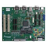
SPC5200CBV400B Freescale Semiconductor, SPC5200CBV400B Datasheet - Page 21

SPC5200CBV400B
Manufacturer Part Number
SPC5200CBV400B
Description
IC MPU 32BIT 500MHZ 272PBGA
Manufacturer
Freescale Semiconductor
Series
MPC603er
Datasheet
1.MPC5200VR400B.pdf
(72 pages)
Specifications of SPC5200CBV400B
Processor Type
MPC52xx PowerPC 32-Bit
Speed
400MHz
Voltage
1.5V
Mounting Type
Surface Mount
Package / Case
272-PBGA
Core Size
32 Bit
Program Memory Size
32KB
Cpu Speed
400MHz
Embedded Interface Type
I2C, SPI, USB
Digital Ic Case Style
BGA
No. Of Pins
272
Rohs Compliant
No
Family Name
MPC52xx
Device Core
PowerPC
Device Core Size
32b
Frequency (max)
400MHz
Instruction Set Architecture
RISC
Supply Voltage 1 (typ)
1.5V
Operating Supply Voltage (max)
1.58V
Operating Supply Voltage (min)
1.42V
Operating Temp Range
-40C to 85C
Operating Temperature Classification
Industrial
Mounting
Surface Mount
Pin Count
272
Package Type
BGA
Lead Free Status / RoHS Status
Lead free / RoHS Compliant
Features
-
Lead Free Status / Rohs Status
Not Compliant
Available stocks
Company
Part Number
Manufacturer
Quantity
Price
Company:
Part Number:
SPC5200CBV400B
Manufacturer:
TOSHIBA
Quantity:
59
Company:
Part Number:
SPC5200CBV400B
Manufacturer:
Freescale Semiconductor
Quantity:
10 000
Part Number:
SPC5200CBV400B
Manufacturer:
FREESCALE
Quantity:
20 000
Company:
Part Number:
SPC5200CBV400BR2
Manufacturer:
Freescale Semiconductor
Quantity:
10 000
1.3.6.4
1.3.7
The PCI interface on the MPC5200B is designed to PCI Version 2.2 and supports 33 MHz and 66 MHz PCI operations. See the
PCI Local Bus Specification; the component section specifies the electrical and timing parameters for PCI components with the
intent that components connect directly together whether on the planar or an expansion board, without any external buffers or
other “glue logic.” Parameters apply at the package pins, not at expansion board edge connectors.
The MPC5200B is always the source of the PCI CLK. The clock waveform must be delivered to each 33 MHz or 66 MHz PCI
component in the system.
environments.
Freescale Semiconductor
data
t
data
mem_clk
t
MDQS (Data Strobe)
Sym
DQSS
NOTE: Control Signals signals are composed of RAS, CAS, MEM_WE, MEM_CS, MEM_CS1, and CLK_EN
valid
hold
Control Signals
PCI
Table 22
MDQ (Data)
Memory Interface Timing-DDR SDRAM Write Command
MEM_CLK
MEM_CLK
Delay from write command to first
MDQ valid before rising edge of
MDQ valid after rising edge of
summarizes the clock specifications.
rising edge of MDQS
MEM_CLK period
Figure 9
Description
Write
MDQS
MDQS
t
DQSS
shows the clock waveform and required measurement points for 3.3 V signaling
Table 21. DDR SDRAM Memory Write Timing
Figure 8. DDR SDRAM Memory Write Timing
datavalid
datahold
MPC5200B Data Sheet, Rev. 4
Write
Min
7.5
1.0
1.0
—
Write
t
mem_clk
Max
—
—
—
Write
+ 0.4
Units
ns
ns
ns
ns
SpecID
A5.20
A5.21
A5.22
A5.23
21


