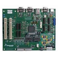
SPC5200CBV400B Freescale Semiconductor, SPC5200CBV400B Datasheet - Page 31

SPC5200CBV400B
Manufacturer Part Number
SPC5200CBV400B
Description
IC MPU 32BIT 500MHZ 272PBGA
Manufacturer
Freescale Semiconductor
Series
MPC603er
Datasheet
1.MPC5200VR400B.pdf
(72 pages)
Specifications of SPC5200CBV400B
Processor Type
MPC52xx PowerPC 32-Bit
Speed
400MHz
Voltage
1.5V
Mounting Type
Surface Mount
Package / Case
272-PBGA
Core Size
32 Bit
Program Memory Size
32KB
Cpu Speed
400MHz
Embedded Interface Type
I2C, SPI, USB
Digital Ic Case Style
BGA
No. Of Pins
272
Rohs Compliant
No
Family Name
MPC52xx
Device Core
PowerPC
Device Core Size
32b
Frequency (max)
400MHz
Instruction Set Architecture
RISC
Supply Voltage 1 (typ)
1.5V
Operating Supply Voltage (max)
1.58V
Operating Supply Voltage (min)
1.42V
Operating Temp Range
-40C to 85C
Operating Temperature Classification
Industrial
Mounting
Surface Mount
Pin Count
272
Package Type
BGA
Lead Free Status / RoHS Status
Lead free / RoHS Compliant
Features
-
Lead Free Status / Rohs Status
Not Compliant
Available stocks
Company
Part Number
Manufacturer
Quantity
Price
Company:
Part Number:
SPC5200CBV400B
Manufacturer:
TOSHIBA
Quantity:
59
Company:
Part Number:
SPC5200CBV400B
Manufacturer:
Freescale Semiconductor
Quantity:
10 000
Part Number:
SPC5200CBV400B
Manufacturer:
FREESCALE
Quantity:
20 000
Company:
Part Number:
SPC5200CBV400BR2
Manufacturer:
Freescale Semiconductor
Quantity:
10 000
Freescale Semiconductor
t
Sym
t
t
t
t
2CYC
t
t
t
CYC
t
DVS
DVH
t
MLI
DH
DMACK
DS
FS
UI
LI
DMARQ
(Drive)
(Host)
RDATA
(Drive)
WDATA
(Host)
DIOR
DIOW
(Host)
Min
114
235
The direction of signal assertion is towards the top of the page, and the direction of negation
is towards the bottom of the page, irrespective of the electrical properties of the signal.
15
70
20
MODE 0
5
6
0
0
0
(ns)
Max
230
150
—
—
—
—
—
—
—
—
Min
156
20
75
10
48
t
MODE 1
5
6
0
0
0
I
t
C
(ns)
Table 29. Ultra DMA Timing Specification
Max
200
150
t
E
—
—
—
—
—
—
—
—
Figure 15. Multiword DMA Timing
t
t
D
G
Min
117
55
34
20
MPC5200B Data Sheet, Rev. 4
MODE 2
7
5
6
0
0
0
(ns)
Max
170 First STROBE time for drive to first negate DSTROBE
150
t
—
—
—
—
—
—
—
t
t
—
F
0
H
NOTE
rising edge to next rising edge or from falling edge to
Data valid hold time at sender, from STROBE edge.
Data valid setup time at sender, to STROBE edge.
variations from STROBE edge to STROBE edge
Two-cycle time allowing for clock variations, from
t
K
Cycle time allowing for asymmetry and clock
from STOP during a data-in burst.
next falling edge of STROBE.
Interlock time with minimum.
Data setup time at recipient.
Data hold time at recipient.
Unlimited interlock time.
Limited Interlock time.
t
L
Comment
t
J
SpecID
A8.26
A8.27
A8.28
A8.29
A8.30
A8.32
A8.33
A8.34
A8.35
A8.31
31


