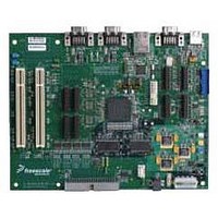
SPC5200CBV400B Freescale Semiconductor, SPC5200CBV400B Datasheet - Page 65

SPC5200CBV400B
Manufacturer Part Number
SPC5200CBV400B
Description
IC MPU 32BIT 500MHZ 272PBGA
Manufacturer
Freescale Semiconductor
Series
MPC603er
Datasheet
1.MPC5200VR400B.pdf
(72 pages)
Specifications of SPC5200CBV400B
Processor Type
MPC52xx PowerPC 32-Bit
Speed
400MHz
Voltage
1.5V
Mounting Type
Surface Mount
Package / Case
272-PBGA
Core Size
32 Bit
Program Memory Size
32KB
Cpu Speed
400MHz
Embedded Interface Type
I2C, SPI, USB
Digital Ic Case Style
BGA
No. Of Pins
272
Rohs Compliant
No
Family Name
MPC52xx
Device Core
PowerPC
Device Core Size
32b
Frequency (max)
400MHz
Instruction Set Architecture
RISC
Supply Voltage 1 (typ)
1.5V
Operating Supply Voltage (max)
1.58V
Operating Supply Voltage (min)
1.42V
Operating Temp Range
-40C to 85C
Operating Temperature Classification
Industrial
Mounting
Surface Mount
Pin Count
272
Package Type
BGA
Lead Free Status / RoHS Status
Lead free / RoHS Compliant
Features
-
Lead Free Status / Rohs Status
Not Compliant
Available stocks
Company
Part Number
Manufacturer
Quantity
Price
Company:
Part Number:
SPC5200CBV400B
Manufacturer:
TOSHIBA
Quantity:
59
Company:
Part Number:
SPC5200CBV400B
Manufacturer:
Freescale Semiconductor
Quantity:
10 000
Part Number:
SPC5200CBV400B
Manufacturer:
FREESCALE
Quantity:
20 000
Company:
Part Number:
SPC5200CBV400BR2
Manufacturer:
Freescale Semiconductor
Quantity:
10 000
The relationship between VDD_IO_MEM and VDD_IO is non-critical during power-up and power-down sequences.
VDD_IO_MEM (2.5 V or 3.3 V) and VDD_IO are specified relative to VDD_CORE.
3.1.1
If VDD_IO/VDD_IO_MEM are powered up with the VDD_CORE at 0 V, the sense circuits in the I/O pads cause all pad output
drivers connected to the VDD_IO/VDD_IO_MEM to be in a high-impedance state. There is no limit to how long after
VDD_IO/VDD_IO_MEM powers up before VDD_CORE must power up. VDD_CORE should not lead the VDD_IO,
VDD_IO_MEM or PLL_AVDD by more than 0.4 V during power ramp up or there will be high current in the internal ESD
protection diodes. The rise times on the power supplies should be slower than 1 microsecond to avoid turning on the internal
ESD protection clamp diodes.
The recommended power up sequence is as follows:
Use one microsecond or slower rise time for all supplies.
VDD_CORE/PLL_AVDD and VDD_IO/VDD_IO_MEM should track up to 0.9 V and then separate for the completion of
ramps with VDD_IO/VDD_IO_MEM going to the higher external voltages. One way to accomplish this is to use a low drop-out
voltage regulator.
3.1.2
If VDD_CORE/PLL_AVDD are powered down first, sense circuits in the I/O pads cause all output drivers to be in a high
impedance state. There is no limit on how long after VDD_CORE and PLL_AVDD power down before VDD_IO or
VDD_IO_MEM must power down. VDD_CORE should not lag VDD_IO, VDD_IO_MEM, or PLL_AVDD going low by more
than 0.5 V during power down or there will be undesired high current in the ESD protection diodes. There are no requirements
for the fall times of the power supplies.
The recommended power down sequence is as follows:
3.2
Each of the independent PLL power supplies require filtering external to the device. The following drawing is a
recommendation for the required filter circuit.
3.3
The MPC5200B requires external pull-up or pull-down resistors on certain pins.
3.3.1
The MPC5200B requires pull-down resistors on the test pins TEST_MODE_0, TEST_MODE_1, TEST_SEL_1.
Freescale Semiconductor
1.
2.
Drop VDD_CORE/PLL_AVDD to 0 V.
Drop VDD_IO/VDD_IO_MEM supplies.
System and CPU Core AVDD Power Supply Filtering
Pull-up/Pull-down Resistor Requirements
Power Up Sequence
Power Down Sequence
Pull-down Resistor Requirements for TEST pins
Power
Supply
source
10 Ω
Figure 52. Power Supply Filtering
10 μF
MPC5200B Data Sheet, Rev. 4
200–400 pF
< 1 Ω
AVDD device pin
65


