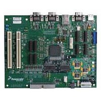
SPC5200CBV400B Freescale Semiconductor, SPC5200CBV400B Datasheet - Page 27

SPC5200CBV400B
Manufacturer Part Number
SPC5200CBV400B
Description
IC MPU 32BIT 500MHZ 272PBGA
Manufacturer
Freescale Semiconductor
Series
MPC603er
Datasheet
1.MPC5200VR400B.pdf
(72 pages)
Specifications of SPC5200CBV400B
Processor Type
MPC52xx PowerPC 32-Bit
Speed
400MHz
Voltage
1.5V
Mounting Type
Surface Mount
Package / Case
272-PBGA
Core Size
32 Bit
Program Memory Size
32KB
Cpu Speed
400MHz
Embedded Interface Type
I2C, SPI, USB
Digital Ic Case Style
BGA
No. Of Pins
272
Rohs Compliant
No
Family Name
MPC52xx
Device Core
PowerPC
Device Core Size
32b
Frequency (max)
400MHz
Instruction Set Architecture
RISC
Supply Voltage 1 (typ)
1.5V
Operating Supply Voltage (max)
1.58V
Operating Supply Voltage (min)
1.42V
Operating Temp Range
-40C to 85C
Operating Temperature Classification
Industrial
Mounting
Surface Mount
Pin Count
272
Package Type
BGA
Lead Free Status / RoHS Status
Lead free / RoHS Compliant
Features
-
Lead Free Status / Rohs Status
Not Compliant
Available stocks
Company
Part Number
Manufacturer
Quantity
Price
Company:
Part Number:
SPC5200CBV400B
Manufacturer:
TOSHIBA
Quantity:
59
Company:
Part Number:
SPC5200CBV400B
Manufacturer:
Freescale Semiconductor
Quantity:
10 000
Part Number:
SPC5200CBV400B
Manufacturer:
FREESCALE
Quantity:
20 000
Company:
Part Number:
SPC5200CBV400BR2
Manufacturer:
Freescale Semiconductor
Quantity:
10 000
1.3.8.3
NOTES:
1. ACK can shorten the CS pulse width.
2. ACK is input and can be used to shorten the CS pulse width.
3. Deadcycles are only used, if no arbitration to an other module (ATA or PCI) of the shared local bus happens. If arbitration
Freescale Semiconductor
Wait States (WS) can be programmed in the Chip Select X Register, Bit field WaitP and WaitX. It can be specified from
0–65535.
happens the bus can be driven within 4 IPB clocks by an other modules.
t
Sym
t
t
t
t
ALEA
t
OEA
OEN
CSA
CSN
TSA
t
t
t
t
t
t
t
t
t
t
t
t
t
t
t
t
10
11
12
13
14
15
16
1
2
3
4
5
6
8
9
7
MUXed Mode
ALE assertion before Address, Bank,
CS assertion before Address, Bank,
RW assertion before ALE assertion
OE assertion before CS assertion
CS assertion before Data wr valid
Data rd setup before CS negation
ACK assertion after CS assertion
OE negation before CS negation
ACK negation after CS negation
CS assertion after TS assertion
RW negation after CS negation
Data wr hold after CS negation
Data rd hold after CS negation
ALE negation to CS assertion
ACK change before PCI clock
ACK change after PCI clock
PCI CLK to ALE assertion
PCI CLK to CS assertion
PCI CLK to CS negation
ALE pulse width
CS pulse width
TSIZ assertion
TS pulse width
TSIZ negation
Description
Table 26. MUXed Mode Timing
MPC5200B Data Sheet, Rev. 4
(2 + WS) × t
t
t
t
IPBIck
IPBIck
IPBIck
Min
4.6
2.9
8.5
—
—
—
—
—
—
—
—
—
—
—
—
—
—
0
PCIck
(DC + 1) × t
(2 + WS) × t
t
t
t
t
t
Max
–1.2
–1.2
10.6
PCIck
PCIck
PCIck
PCIck
PCIck
7.0
3.6
5.7
6.9
4.7
5.9
2.0
4.4
—
—
—
—
PCIck
PCIck
Units
ns
ns
ns
ns
ns
ns
ns
ns
ns
ns
ns
ns
ns
ns
ns
ns
ns
ns
ns
ns
ns
ns
Notes SpecID
(1),(3)
—
—
—
—
—
—
—
—
—
—
—
—
—
—
—
—
(2)
(2)
(2)
(2)
A7.39
A7.40
A7.41
A7.42
A7.43
A7.44
A7.45
A7.46
A7.47
A7.48
A7.49
A7.50
A7.51
A7.52
A7.53
A7.54
A7.55
A7.56
A7.57
A7.58
A7.59
A7.60
27


