MPC8321CVRAFDC Freescale Semiconductor, MPC8321CVRAFDC Datasheet - Page 10
MPC8321CVRAFDC
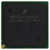
Manufacturer Part Number
MPC8321CVRAFDC
Description
IC MPU PWRQUICC II 516-PBGA
Manufacturer
Freescale Semiconductor
Datasheet
1.MPC8321VRADDC.pdf
(82 pages)
Specifications of MPC8321CVRAFDC
Processor Type
MPC83xx PowerQUICC II Pro 32-Bit
Speed
333MHz
Voltage
1V
Mounting Type
Surface Mount
Package / Case
516-PBGA
Processor Series
MPC8xxx
Core
e300
Data Bus Width
32 bit
Development Tools By Supplier
MPC8323E-MDS-PB
Maximum Clock Frequency
333 MHz
Maximum Operating Temperature
+ 105 C
Mounting Style
SMD/SMT
Data Ram Size
16 KB
I/o Voltage
1.8 V, 3.3 V
Interface Type
I2C, SPI, UART
Minimum Operating Temperature
- 40 C
Leaded Process Compatible
Yes
Rohs Compliant
Yes
Peak Reflow Compatible (260 C)
Yes
Lead Free Status / RoHS Status
Lead free / RoHS Compliant
Features
-
Lead Free Status / Rohs Status
Lead free / RoHS Compliant
Available stocks
Company
Part Number
Manufacturer
Quantity
Price
Company:

Part Number:
MPC8321CVRAFDC
Manufacturer:
CPClare
Quantity:
672
Company:
Part Number:
MPC8321CVRAFDC
Manufacturer:
Freescale Semiconductor
Quantity:
10 000
Part Number:
MPC8321CVRAFDC
Manufacturer:
FREESCALE
Quantity:
20 000


Local bus I/O
load = 25 pF
1 pair of clocks
PCI I/O load = 30 pF
QUICC Engine block and
other I/Os
Clock Input Timing
4
This section provides the clock input DC and AC electrical characteristics for the MPC8323E.
4.1
Table 7
10
Input high voltage
Input low voltage
MPC8323E PowerQUICC II Pro Integrated Communications Processor Family Hardware Specifications, Rev. 4
Clock Input Timing
provides the clock input (CLKIN/PCI_SYNC_IN) DC timing specifications for the MPC8323E.
DC Electrical Characteristics
Parameter
AV
conditions and ambient temperature).
The rise/fall time on QUICC Engine input pins should not exceed 5 ns. This
should be enforced especially on clock signals. Rise time refers to signal
transitions from 10% to 90% of VCC; fall time refers to transitions from
90% to 10% of VCC.
DD
n (1.0 V) is estimated to consume 0.05 W (under normal operating
Table 6. Estimated Typical I/O Power Dissipation (continued)
66 MHz, 32 bits
66 MHz, 32 bits
UTOPIA 8-bit 31 PHYs
TDM serial
TDM nibble
HDLC/TRAN serial
HDLC/TRAN nibble
DUART
MIIs
RMII
Ethernet management
USB
SPI
Timer output
Table 7. CLKIN DC Electrical Characteristics
Condition
—
—
NOTE
NOTE
—
—
—
—
—
—
—
—
—
—
—
—
—
—
Symbol
V
V
IH
IL
—
—
—
—
—
—
—
—
—
—
—
—
—
—
–0.3
Min
2.7
0.057
0.041
0.001
0.004
0.003
0.025
0.017
0.009
0.009
0.002
0.001
0.001
0.002
0.12
Freescale Semiconductor
OV
W
W
W
W
W
W
W
W
W
W
W
W
W
W
DD
Max
0.4
+ 0.3
Multiply by
number of
interfaces used.
—
—
Unit
V
V
Related parts for MPC8321CVRAFDC
Image
Part Number
Description
Manufacturer
Datasheet
Request
R

Part Number:
Description:
Manufacturer:
Freescale Semiconductor, Inc
Datasheet:
Part Number:
Description:
Manufacturer:
Freescale Semiconductor, Inc
Datasheet:
Part Number:
Description:
Manufacturer:
Freescale Semiconductor, Inc
Datasheet:
Part Number:
Description:
Manufacturer:
Freescale Semiconductor, Inc
Datasheet:
Part Number:
Description:
Manufacturer:
Freescale Semiconductor, Inc
Datasheet:
Part Number:
Description:
Manufacturer:
Freescale Semiconductor, Inc
Datasheet:
Part Number:
Description:
Manufacturer:
Freescale Semiconductor, Inc
Datasheet:
Part Number:
Description:
Manufacturer:
Freescale Semiconductor, Inc
Datasheet:
Part Number:
Description:
Manufacturer:
Freescale Semiconductor, Inc
Datasheet:
Part Number:
Description:
Manufacturer:
Freescale Semiconductor, Inc
Datasheet:
Part Number:
Description:
Manufacturer:
Freescale Semiconductor, Inc
Datasheet:
Part Number:
Description:
Manufacturer:
Freescale Semiconductor, Inc
Datasheet:
Part Number:
Description:
Manufacturer:
Freescale Semiconductor, Inc
Datasheet:
Part Number:
Description:
Manufacturer:
Freescale Semiconductor, Inc
Datasheet:
Part Number:
Description:
Manufacturer:
Freescale Semiconductor, Inc
Datasheet: