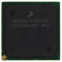
MPC8321CVRAFDC Freescale Semiconductor, MPC8321CVRAFDC Datasheet - Page 78

MPC8321CVRAFDC
Manufacturer Part Number
MPC8321CVRAFDC
Description
IC MPU PWRQUICC II 516-PBGA
Manufacturer
Freescale Semiconductor
Datasheet
1.MPC8321VRADDC.pdf
(82 pages)
Specifications of MPC8321CVRAFDC
Processor Type
MPC83xx PowerQUICC II Pro 32-Bit
Speed
333MHz
Voltage
1V
Mounting Type
Surface Mount
Package / Case
516-PBGA
Processor Series
MPC8xxx
Core
e300
Data Bus Width
32 bit
Development Tools By Supplier
MPC8323E-MDS-PB
Maximum Clock Frequency
333 MHz
Maximum Operating Temperature
+ 105 C
Mounting Style
SMD/SMT
Data Ram Size
16 KB
I/o Voltage
1.8 V, 3.3 V
Interface Type
I2C, SPI, UART
Minimum Operating Temperature
- 40 C
Leaded Process Compatible
Yes
Rohs Compliant
Yes
Peak Reflow Compatible (260 C)
Yes
Lead Free Status / RoHS Status
Lead free / RoHS Compliant
Features
-
Lead Free Status / Rohs Status
Lead free / RoHS Compliant
Available stocks
Company
Part Number
Manufacturer
Quantity
Price
Company:
Part Number:
MPC8321CVRAFDC
Manufacturer:
CPClare
Quantity:
672
Company:
Part Number:
MPC8321CVRAFDC
Manufacturer:
Freescale Semiconductor
Quantity:
10 000
Part Number:
MPC8321CVRAFDC
Manufacturer:
FREESCALE
Quantity:
20 000
System Design Information
output impedance is the average of two components, the resistances of the pull-up and pull-down devices.
When data is held high, SW1 is closed (SW2 is open) and R
OV
other in value. Then, Z
The value of this resistance and the strength of the driver’s current source can be found by making two
measurements. First, the output voltage is measured while driving logic 1 without an external differential
termination resistor. The measured voltage is V
while driving logic 1 with an external precision differential termination resistor of value R
measured voltage is V
R
Table 65
nominal OV
24.6
The MPC8323E provides the user with power-on configuration options which can be set through the use
of external pull-up or pull-down resistors of 4.7 kΩ on certain output pins (see customer visible
configuration pins). These pins are generally used as output only pins in normal operation.
78
Note: Nominal supply voltages. See
term
Impedance
Differential
DD
MPC8323E PowerQUICC II Pro Integrated Communications Processor Family Hardware Specifications, Rev. 4
× (V
R
R
/2. R
N
P
summarizes the signal impedance targets. The driver impedance are targeted at minimum V
Configuration Pin Multiplexing
1
P
/V
DD
then becomes the resistance of the pull-up devices. R
2
, 105°C.
– 1). The drive current is then I
Local Bus, Ethernet, DUART, Control,
Configuration, Power Management
2
0
= (1/(1/R
= (R
42 Target
42 Target
P
+ R
Table
NA
Figure 45. Driver Impedance Measurement
1
Data
N
+ 1/R
Table 65. Impedance Characteristics
)/2.
1, T
j
= 105°C.
2
)) × I
1
source
source
= R
source
. Solving for the output impedance gives R
= V
25 Target
25 Target
PCI
NA
1
× I
/R
P
Pad
source
R
R
source
is trimmed until the voltage at the pad equals
N
P
OGND
OV
DD
P
. Second, the output voltage is measured
.
and R
SW2
SW1
DDR DRAM
20 Target
20 Target
N
NA
are designed to be close to each
Freescale Semiconductor
Symbol
Z
Z
Z
DIFF
0
0
term
. The
source
Unit
W
W
W
=
DD
,


