MPC8321CVRAFDC Freescale Semiconductor, MPC8321CVRAFDC Datasheet - Page 22
MPC8321CVRAFDC
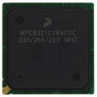
Manufacturer Part Number
MPC8321CVRAFDC
Description
IC MPU PWRQUICC II 516-PBGA
Manufacturer
Freescale Semiconductor
Datasheet
1.MPC8321VRADDC.pdf
(82 pages)
Specifications of MPC8321CVRAFDC
Processor Type
MPC83xx PowerQUICC II Pro 32-Bit
Speed
333MHz
Voltage
1V
Mounting Type
Surface Mount
Package / Case
516-PBGA
Processor Series
MPC8xxx
Core
e300
Data Bus Width
32 bit
Development Tools By Supplier
MPC8323E-MDS-PB
Maximum Clock Frequency
333 MHz
Maximum Operating Temperature
+ 105 C
Mounting Style
SMD/SMT
Data Ram Size
16 KB
I/o Voltage
1.8 V, 3.3 V
Interface Type
I2C, SPI, UART
Minimum Operating Temperature
- 40 C
Leaded Process Compatible
Yes
Rohs Compliant
Yes
Peak Reflow Compatible (260 C)
Yes
Lead Free Status / RoHS Status
Lead free / RoHS Compliant
Features
-
Lead Free Status / Rohs Status
Lead free / RoHS Compliant
Available stocks
Company
Part Number
Manufacturer
Quantity
Price
Company:

Part Number:
MPC8321CVRAFDC
Manufacturer:
CPClare
Quantity:
672
Company:
Part Number:
MPC8321CVRAFDC
Manufacturer:
Freescale Semiconductor
Quantity:
10 000
Part Number:
MPC8321CVRAFDC
Manufacturer:
FREESCALE
Quantity:
20 000


Ethernet and MII Management
Figure 8
Figure 9
8.2.2
This section describes the RMII transmit and receive AC timing specifications.
22
At recommended operating conditions with OV
RX_CLK clock fall time
Note:
1. The symbols used for timing specifications follow the pattern of t
inputs and t
timing (MR) with respect to the time data input signals (D) reach the valid state (V) relative to the t
going to the high (H) state or setup time. Also, t
signals (D) went invalid (X) relative to the t
the clock reference symbol representation is based on three letters representing the clock of a particular functional. For
example, the subscript of t
with the appropriate letter: R (rise) or F (fall).
MPC8323E PowerQUICC II Pro Integrated Communications Processor Family Hardware Specifications, Rev. 4
provides the AC test load.
shows the MII receive AC timing diagram.
RMII AC Timing Specifications
(first two letters of functional block)(reference)(state)(signal)(state)
RXD[3:0]
RX_CLK
Parameter/Condition
RX_DV
RX_ER
Output
Table 24. MII Receive AC Timing Specifications (continued)
MRX
represents the MII (M) receive (RX) clock. For rise and fall times, the latter convention is used
t
Figure 9. MII Receive AC Timing Diagram
t
MRXH
MRDVKH
DD
of 3.3 V ± 10%.
MRX
t
MRX
Z
clock reference (K) going to the low (L) state or hold time. Note that, in general,
MRDXKL
Figure 8. AC Test Load
0
= 50 Ω
Valid Data
symbolizes MII receive timing (GR) with respect to the time data input
t
Symbol
MRXF
t
(first two letters of functional block)(signal)(state)(reference)(state)
MRXF
for outputs. For example, t
1
R
L
t
MRDXKH
t
= 50 Ω
MRXR
Min
1.0
OV
DD
Typical
MRDVKH
/2
—
MRX
Freescale Semiconductor
symbolizes MII receive
clock reference (K)
Max
4.0
Unit
ns
for
Related parts for MPC8321CVRAFDC
Image
Part Number
Description
Manufacturer
Datasheet
Request
R

Part Number:
Description:
Manufacturer:
Freescale Semiconductor, Inc
Datasheet:
Part Number:
Description:
Manufacturer:
Freescale Semiconductor, Inc
Datasheet:
Part Number:
Description:
Manufacturer:
Freescale Semiconductor, Inc
Datasheet:
Part Number:
Description:
Manufacturer:
Freescale Semiconductor, Inc
Datasheet:
Part Number:
Description:
Manufacturer:
Freescale Semiconductor, Inc
Datasheet:
Part Number:
Description:
Manufacturer:
Freescale Semiconductor, Inc
Datasheet:
Part Number:
Description:
Manufacturer:
Freescale Semiconductor, Inc
Datasheet:
Part Number:
Description:
Manufacturer:
Freescale Semiconductor, Inc
Datasheet:
Part Number:
Description:
Manufacturer:
Freescale Semiconductor, Inc
Datasheet:
Part Number:
Description:
Manufacturer:
Freescale Semiconductor, Inc
Datasheet:
Part Number:
Description:
Manufacturer:
Freescale Semiconductor, Inc
Datasheet:
Part Number:
Description:
Manufacturer:
Freescale Semiconductor, Inc
Datasheet:
Part Number:
Description:
Manufacturer:
Freescale Semiconductor, Inc
Datasheet:
Part Number:
Description:
Manufacturer:
Freescale Semiconductor, Inc
Datasheet:
Part Number:
Description:
Manufacturer:
Freescale Semiconductor, Inc
Datasheet: