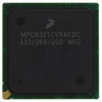
MPC8321CVRAFDC Freescale Semiconductor, MPC8321CVRAFDC Datasheet - Page 9

MPC8321CVRAFDC
Manufacturer Part Number
MPC8321CVRAFDC
Description
IC MPU PWRQUICC II 516-PBGA
Manufacturer
Freescale Semiconductor
Datasheet
1.MPC8321VRADDC.pdf
(82 pages)
Specifications of MPC8321CVRAFDC
Processor Type
MPC83xx PowerQUICC II Pro 32-Bit
Speed
333MHz
Voltage
1V
Mounting Type
Surface Mount
Package / Case
516-PBGA
Processor Series
MPC8xxx
Core
e300
Data Bus Width
32 bit
Development Tools By Supplier
MPC8323E-MDS-PB
Maximum Clock Frequency
333 MHz
Maximum Operating Temperature
+ 105 C
Mounting Style
SMD/SMT
Data Ram Size
16 KB
I/o Voltage
1.8 V, 3.3 V
Interface Type
I2C, SPI, UART
Minimum Operating Temperature
- 40 C
Leaded Process Compatible
Yes
Rohs Compliant
Yes
Peak Reflow Compatible (260 C)
Yes
Lead Free Status / RoHS Status
Lead free / RoHS Compliant
Features
-
Lead Free Status / Rohs Status
Lead free / RoHS Compliant
Available stocks
Company
Part Number
Manufacturer
Quantity
Price
Company:
Part Number:
MPC8321CVRAFDC
Manufacturer:
CPClare
Quantity:
672
Company:
Part Number:
MPC8321CVRAFDC
Manufacturer:
Freescale Semiconductor
Quantity:
10 000
Part Number:
MPC8321CVRAFDC
Manufacturer:
FREESCALE
Quantity:
20 000
DDR I/O
65% utilization
2.5 V
R
R
1 pair of clocks
3
The estimated typical power dissipation for this family of MPC8323E devices is shown in
Table 6
Freescale Semiconductor
Notes:
1. The values do not include I/O supply power (OV
2. Typical power is based on a nominal voltage of V
3. Maximum power is based on a voltage of V
s
t
= 50 Ω
Frequency (MHz)
= 20 Ω
benchmark application. The measurements were taken on the MPC8323MDS evaluation board using WC process silicon.
MPC8323E PowerQUICC II Pro Integrated Communications Processor Family Hardware Specifications, Rev. 4
Interface
Power Characteristics
CSB
shows the estimated typical I/O power dissipation for the device.
133
133
90%
V
Frequency (MHz)
0
QUICC Engine
266 MHz, 1 × 32 bits
PORESET
Figure 3. MPC8323E Power-Up Sequencing Example
200
200
Table 6. Estimated Typical I/O Power Dissipation
Parameter
Table 5. MPC8323E Power Dissipation
DD
= 1.07 V, WC process, a junction T
Frequency (MHz)
DD
DD
and GV
= 1.0 V, ambient temperature, and the core running a Dhrystone
Core
GV
266
333
DD
0.212
DD
(1.8 V)
) or AV
I/O Voltage (GV
>= 32 clocks x t
DD
GV
. For I/O power values, see
Typical
Core Voltage (V
DD
0.74
0.78
0.367
(2.5 V) OV
DD
SYS_CLK_IN
J
and OV
= 110°C, and an artificial smoke test.
Maximum
DD
DD
1.48
1.62
DD
—
)
0.7 V
/t
(3.3 V) Unit
PCI_SYNC_IN
)
Table
t
W
Power Characteristics
Unit
W
W
6.
Table
Comments
—
5.
Notes
1, 2, 3
1, 2, 3
9


