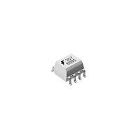
HUF76131SK8 Fairchild Semiconductor, HUF76131SK8 Datasheet - Page 7

HUF76131SK8
Manufacturer Part Number
HUF76131SK8
Description
MOSFET Power 10a 30V 0.013 Ohm 1Ch HS Logic Gate
Manufacturer
Fairchild Semiconductor
Specifications of HUF76131SK8
Configuration
Single Quad Drain Triple Source
Transistor Polarity
N-Channel
Resistance Drain-source Rds (on)
0.013 Ohms
Drain-source Breakdown Voltage
30 V
Gate-source Breakdown Voltage
+/- 20 V
Continuous Drain Current
10 A
Power Dissipation
2.5 W
Maximum Operating Temperature
+ 150 C
Mounting Style
SMD/SMT
Package / Case
SOP-8
Minimum Operating Temperature
- 55 C
Lead Free Status / Rohs Status
No
Available stocks
Company
Part Number
Manufacturer
Quantity
Price
Part Number:
HUF76131SK8T
Manufacturer:
INFINEON/英飞凌
Quantity:
20 000
Thermal Resistance vs Mounting Pad Area
The maximum rated junction temperature T
the maximum allowable device power dissipation P
an application. The application ambient temperature T
and thermal impedance Z
ensure that T
mathematically represents the relationship.
Fairchild provides thermal information to assist the
designer’s preliminary application evaluation. Precise
determination of P
factors:
Figure 22 addresses these points by depicting R
vs. top copper (component side) heat sink area. The
measurements were performed in still air using a horizontally
positioned FR-4 board with 1oz copper after 1000 seconds
of steady state power.
Figure 22 also displays the two R
Electrical Specifications table. The two points were chosen
to graphically depict the compromise between copper board
area, thermal resistance and ultimately power dissipation.
©2003 Fairchild Semiconductor Corporation
P DMAX
1. PC heat sink area and location (top and bottom), copper
2. Air Flow, board orientation and type.
3. Power pulse width and duty factor.
leads and mounting pad area.
=
--------------------------------------- -
T
JMAX
JMAX
Z JA
–
DMAX
T
(
A
o
C) is never exceeded. Equation 1
is complex and influenced by many
JA
(
o
C/W) must be reviewed to
JA
values listed in the
JMAX
constrains
JA
Dmax
values
A
(EQ. 1)
(
o
in
C)
Thermal resistance values corresponding to other
component side copper areas can be obtained from Figure
22 or by calculation using Equation 2. Area in Equation 2 is
the top copper area including the gate and source pads.
FIGURE 22. THERMAL RESISTANCE vs MOUNTING PAD AREA
Figure 22 provides the necessary information for steady
state junction temperature or power dissipation calculations.
Transient pulse applications are best studied using the
Fairchild device SPICE thermal model.
R
JA
250
200
150
100
50
=
0.001
79.3 21.8
–
AREA, TOP COPPER AREA (in
ln
Area
0.01
177.3
o
C/W - 0.0115in
R
JA
143.4
= 79.3 - 21.8
0.1
o
C/W - 0.054in
HUF76131SK8 Rev. B1
2
2
)
*
ln(AREA)
(EQ. 2)
2
1.0


