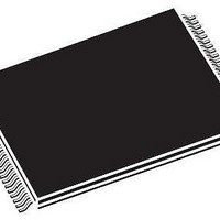
M29W320DT70N6 STMicroelectronics, M29W320DT70N6 Datasheet - Page 12

M29W320DT70N6
Manufacturer Part Number
M29W320DT70N6
Description
Flash 4Mx8 or 2Mx16 70ns
Manufacturer
STMicroelectronics
Datasheet
1.M29W320DT70N6.pdf
(46 pages)
Specifications of M29W320DT70N6
Data Bus Width
8 bit, 16 bit
Memory Type
NOR Flash
Memory Size
32 Mbit
Architecture
Sectored
Interface Type
CFI
Access Time
70 ns
Supply Voltage (max)
3.6 V
Supply Voltage (min)
2.7 V
Maximum Operating Current
10 mA
Operating Temperature
+ 85 C
Mounting Style
SMD/SMT
Package / Case
TSOP-1-48
Organization
4 MB x 8
Lead Free Status / Rohs Status
Details
Available stocks
Company
Part Number
Manufacturer
Quantity
Price
Company:
Part Number:
M29W320DT70N6
Manufacturer:
ST
Quantity:
3 000
Company:
Part Number:
M29W320DT70N6
Manufacturer:
ST
Quantity:
3 000
Part Number:
M29W320DT70N6
Manufacturer:
ST
Quantity:
20 000
Company:
Part Number:
M29W320DT70N6
Manufacturer:
ST
Quantity:
12 103
Company:
Part Number:
M29W320DT70N6E
Manufacturer:
ST
Quantity:
1 500
Company:
Part Number:
M29W320DT70N6E
Manufacturer:
ST
Quantity:
3 198
Company:
Part Number:
M29W320DT70N6E
Manufacturer:
ST
Quantity:
3 198
Part Number:
M29W320DT70N6E
Manufacturer:
MICRON/ST
Quantity:
20 000
M29W320DT, M29W320DB
Note that if V
outermost boot block will remain protect even if RP
is at V
After a Hardware Reset, Bus Read and Bus Write
operations cannot begin until Ready/Busy be-
comes high-impedance. See Table 14. and Figure
Figure 16., Reset/Temporary Unprotect AC Char-
acteristics.
The use of an open-drain output allows the Ready/
Busy pins from several memories to be connected
to a single pull-up resistor. A Low will then indicate
that one, or more, of the memories is busy.
Byte/Word Organization Select (BYTE). The
Byte/Word Organization Select pin is used to
switch between the x8 and x16 Bus modes of the
memory. When Byte/Word Organization Select is
Low, V
High, V
12/46
ID
IL
IH
.
, the memory is in x8 mode, when it is
, the memory is in x16 mode.
PP
/WP is at V
IL
, then the 16 KByte
V
vides the power supply for all operations (Read,
Program and Erase).
The Command Interface is disabled when the V
Supply Voltage is less than the Lockout Voltage,
V
cidentally damaging the data during power up,
power down and power surges. If the Program/
Erase Controller is programming or erasing during
this time then the operation aborts and the memo-
ry contents being altered will be invalid.
A 0.1µF capacitor should be connected between
the V
pin to decouple the current surges from the power
supply. The PCB track widths must be sufficient to
carry the currents required during Program and
Erase operations, I
V
measurements.
CC
LKO
SS
Ground. V
Supply Voltage (2.7V to 3.6V). V
. This prevents Bus Write operations from ac-
CC
Supply Voltage pin and the V
SS
CC3
is the reference for all voltage
.
SS
CC
Ground
pro-
CC


