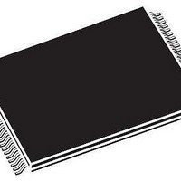
M29W320DT70N6 STMicroelectronics, M29W320DT70N6 Datasheet - Page 21

M29W320DT70N6
Manufacturer Part Number
M29W320DT70N6
Description
Flash 4Mx8 or 2Mx16 70ns
Manufacturer
STMicroelectronics
Datasheet
1.M29W320DT70N6.pdf
(46 pages)
Specifications of M29W320DT70N6
Data Bus Width
8 bit, 16 bit
Memory Type
NOR Flash
Memory Size
32 Mbit
Architecture
Sectored
Interface Type
CFI
Access Time
70 ns
Supply Voltage (max)
3.6 V
Supply Voltage (min)
2.7 V
Maximum Operating Current
10 mA
Operating Temperature
+ 85 C
Mounting Style
SMD/SMT
Package / Case
TSOP-1-48
Organization
4 MB x 8
Lead Free Status / Rohs Status
Details
Available stocks
Company
Part Number
Manufacturer
Quantity
Price
Company:
Part Number:
M29W320DT70N6
Manufacturer:
ST
Quantity:
3 000
Company:
Part Number:
M29W320DT70N6
Manufacturer:
ST
Quantity:
3 000
Part Number:
M29W320DT70N6
Manufacturer:
ST
Quantity:
20 000
Company:
Part Number:
M29W320DT70N6
Manufacturer:
ST
Quantity:
12 103
Company:
Part Number:
M29W320DT70N6E
Manufacturer:
ST
Quantity:
1 500
Company:
Part Number:
M29W320DT70N6E
Manufacturer:
ST
Quantity:
3 198
Company:
Part Number:
M29W320DT70N6E
Manufacturer:
ST
Quantity:
3 198
Part Number:
M29W320DT70N6E
Manufacturer:
MICRON/ST
Quantity:
20 000
before other commands are issued. The Error bit
is output on DQ5 when the Status Register is read.
Note that the Program command cannot change a
bit set to ’0’ back to ’1’ and attempting to do so will
set DQ5 to ‘1’. A Bus Read operation to that ad-
dress will show the bit is still ‘0’. One of the Erase
commands must be used to set all the bits in a
block or in the whole memory from ’0’ to ’1’.
Erase Timer Bit (DQ3). The Erase Timer Bit can
be used to identify the start of Program/Erase
Controller operation during a Block Erase com-
mand. Once the Program/Erase Controller starts
erasing the Erase Timer Bit is set to ’1’. Before the
Program/Erase Controller starts the Erase Timer
Bit is set to ’0’ and additional blocks to be erased
may be written to the Command Interface. The
Erase Timer Bit is output on DQ3 when the Status
Register is read.
Alternative Toggle Bit (DQ2). The
Toggle Bit can be used to monitor the Program/
Erase controller during Erase operations. The Al-
ternative Toggle Bit is output on DQ2 when the
Status Register is read.
Table 6. Status Register Bits
Note: Unspecified data bits should be ignored.
Program
Program During Erase
Suspend
Program Error
Chip Erase
Block Erase before
timeout
Block Erase
Erase Suspend
Erase Error
Operation
Faulty Block Address
Good Block Address
Non-Erasing Block
Non-Erasing Block
Non-Erasing Block
Erasing Block
Erasing Block
Erasing Block
Any Address
Any Address
Any Address
Any Address
Address
Alternative
DQ7
DQ7
DQ7
DQ7
0
0
0
0
0
1
0
0
During Chip Erase and Block Erase operations the
Toggle Bit changes from ’0’ to ’1’ to ’0’, etc., with
successive Bus Read operations from addresses
within the blocks being erased. A protected block
is treated the same as a block not being erased.
Once the operation completes the memory returns
to Read mode.
During Erase Suspend the Alternative Toggle Bit
changes from ’0’ to ’1’ to ’0’, etc. with successive
Bus Read operations from addresses within the
blocks being erased. Bus Read operations to ad-
dresses within blocks not being erased will output
the memory cell data as if in Read mode.
After an Erase operation that causes the Error Bit
to be set the Alternative Toggle Bit can be used to
identify which block or blocks have caused the er-
ror. The Alternative Toggle Bit changes from ’0’ to
’1’ to ’0’, etc. with successive Bus Read Opera-
tions from addresses within blocks that have not
erased correctly. The Alternative Toggle Bit does
not change if the addressed block has erased cor-
rectly.
No Toggle
Toggle
Toggle
Toggle
Toggle
Toggle
Toggle
Toggle
Toggle
Toggle
Toggle
DQ6
Data read as normal
DQ5
0
0
1
0
0
0
0
0
0
1
1
M29W320DT, M29W320DB
DQ3
–
–
–
1
0
0
1
1
–
1
1
No Toggle
No Toggle
No Toggle
Toggle
Toggle
Toggle
Toggle
Toggle
DQ2
–
–
–
RB
0
0
0
0
0
0
0
0
1
1
0
0
21/46


