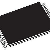
M29W320DT70N6 STMicroelectronics, M29W320DT70N6 Datasheet - Page 45

M29W320DT70N6
Manufacturer Part Number
M29W320DT70N6
Description
Flash 4Mx8 or 2Mx16 70ns
Manufacturer
STMicroelectronics
Datasheet
1.M29W320DT70N6.pdf
(46 pages)
Specifications of M29W320DT70N6
Data Bus Width
8 bit, 16 bit
Memory Type
NOR Flash
Memory Size
32 Mbit
Architecture
Sectored
Interface Type
CFI
Access Time
70 ns
Supply Voltage (max)
3.6 V
Supply Voltage (min)
2.7 V
Maximum Operating Current
10 mA
Operating Temperature
+ 85 C
Mounting Style
SMD/SMT
Package / Case
TSOP-1-48
Organization
4 MB x 8
Lead Free Status / Rohs Status
Details
Available stocks
Company
Part Number
Manufacturer
Quantity
Price
Company:
Part Number:
M29W320DT70N6
Manufacturer:
ST
Quantity:
3 000
Company:
Part Number:
M29W320DT70N6
Manufacturer:
ST
Quantity:
3 000
Part Number:
M29W320DT70N6
Manufacturer:
ST
Quantity:
20 000
Company:
Part Number:
M29W320DT70N6
Manufacturer:
ST
Quantity:
12 103
Company:
Part Number:
M29W320DT70N6E
Manufacturer:
ST
Quantity:
1 500
Company:
Part Number:
M29W320DT70N6E
Manufacturer:
ST
Quantity:
3 198
Company:
Part Number:
M29W320DT70N6E
Manufacturer:
ST
Quantity:
3 198
Part Number:
M29W320DT70N6E
Manufacturer:
MICRON/ST
Quantity:
20 000
REVISION HISTORY
Table 28. Document Revision History
26-May-2003
19-Nov-2002
16-Aug-2005
07-Feb-2002
08-Jun-2001
22-Jun-2001
05-Oct-2001
05-Apr-2002
March-2001
27-Jul-2001
Date
Version
-01
-02
-03
-04
-05
-06
-07
7.1
7.2
8.0
First Issue (Brief Data)
Document expanded to full Product Preview
Minor text corrections to Read/Reset and Read CFI commands and Status Register Error
and Toggle Bits.
Document type: from Product Preview to Preliminary Data
TFBGA connections and Block Addresses (x16) diagrams clarification
Write Protect and Block Unprotect clarification
CFI Primary Algorithm table, Block Protection change
Added Block Protection Appendix
“Write Protect/V
Changes to the V
Table 10. and I
Command section. Added V
Clarified Read/Reset operation during Erase Suspend.
TFBGA package changed from 48 ball to 63 ball
Description of Ready/Busy signal clarified (and Figure 16 modified)
Clarified allowable commands during block erase
Clarified the mode the device returns to in the CFI Read Query command section
Erase Suspend Latency Time (typical and maximum) added to Program, Erase Times
and Program, Erase Endurance Cycles table.
Typical values added for Icc1 and Icc2 in DC characteristics table.
Logic Diagram and Data Toggle Flowchart corrected.
Revision numbering modified: a minor revision will be indicated by incrementing the digit
after the dot, and a major revision, by incrementing the digit before the dot (revision
version 07 equals 7.0). Document promoted to full datasheet.
Data Retention added to Table 5., Program, Erase Times and Program, Erase Endurance
Cycles, and Typical after 100k W/E Cycles column removed. TSOP48 package
mechanical updated. Lead-free package options E and F added to Table 18., Ordering
Information Scheme.
TFBGA48 package added throughout document.
CC3
PP
PP
” pin renamed to “V
clarified. Modified description of V
/WP pin description, Figure Figure 17. and Table 14.. I
PP
/WP decoupling capacitor to Figure Figure 12..
Revision Details
PP
/Write Protect” to be consistent with abbreviation.
PP
M29W320DT, M29W320DB
/WP operation in Unlock Bypass
PP
added to
45/46


