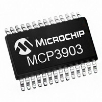
MCP3903-I/SS Microchip Technology, MCP3903-I/SS Datasheet - Page 30

MCP3903-I/SS
Manufacturer Part Number
MCP3903-I/SS
Description
IC AFE 24BIT 64KSPS 28SSOP
Manufacturer
Microchip Technology
Series
-r
Datasheet
1.MCP3903-ISS.pdf
(54 pages)
Specifications of MCP3903-I/SS
Featured Product
MCP3903 Six Channel ÎΣ A/D Converter
Number Of Bits
24
Number Of Channels
6
Power (watts)
-
Voltage - Supply, Analog
4.5 V ~ 5.5 V
Voltage - Supply, Digital
2.7 V ~ 3.6 V
Package / Case
28-SSOP (0.209", 5.30mm Width)
Lead Free Status / Rohs Status
Lead free / RoHS Compliant
Available stocks
Company
Part Number
Manufacturer
Quantity
Price
Company:
Part Number:
MCP3903-I/SS
Manufacturer:
Microchip
Quantity:
263
Part Number:
MCP3903-I/SS
Manufacturer:
MICROCHIP/微芯
Quantity:
20 000
MCP3903
6.0
6.1
The MCP3903 device is compatible with SPI modes
0,0 and 1,1. Data is clocked out of the MCP3903 on the
falling edge of SCK, and data is clocked into the
MCP3903 on the rising edge of SCK. In these modes,
SCK can idle either high or low. Each SPI
communication starts with a CS falling edge and stops
with the CS rising edge. Each SPI communication is
independent. When CS is high, SDO is in high
impedance, and transitions on SCK and SDI have no
effect. Additional controls: RESET, DR are also
provided
communication. The MCP3903 interface has a simple
command structure. The first byte transmitted is always
the CONTROL byte that is 8 bits wide and is followed
by data bytes that are 24 bits wide. Both ADCs are
continuously converting data by default and can be
reset or shutdown through a CONFIG register setting.
Since each ADC data is either 16 or 24 bits (depending
on the WIDTH bits), the internal registers can be
grouped together with various configurations (through
the READ bits) in order to allow easy data retrieval
within only one communication. For device reads, the
internal address counter can be automatically incre-
mented in order to loop through groups of data within
the register map. The SDO will then output the data
located at the ADDRESS (A<4:0>) defined in the con-
trol byte and then ADDRESS+1 depending on the
READ<1:0> bits which select the groups of registers.
These groups are defined in Section 7.1 “ADC Chan-
nel Data Output Registers” (Register Map). The Data
Ready pins (DRn) can be used as an interrupt for an
MCU and outputs pulses when new ADC channel data
is available. The RESET pin acts like a hard reset and
can reset the part to its default power-up configuration.
6.2
The control byte of the MCP3903 contains two device
address bits A<6:5>, 5 register address bits A<4:0>,
and a read/write bit (R/W). The first byte transmitted to
the MCP3903 is always the control byte.
FIGURE 6-1:
DS25048B-page 30
Address Bits
A6
(0)
Device
DESCRIPTION
OVERVIEW
CONTROL BYTE
SERIAL INTERFACE
A5
(1)
on
A4
separate
A3
Control Byte.
Address Bits
Register
A2
pins
A1 A0
for
R/W
Write Bit
Read
advanced
The default device address bits are 01. A read on
undefined addresses will give an all zeros output on the
first and all subsequent transmitted bytes. A write on an
undefined address will have no effect and will not incre-
ment the address counter either.
The register map is defined in Section 7.1 “ADC
Channel Data Output Registers”.
6.3
The first data byte read is the one defined by the
address given in the CONTROL byte. After this first
byte is transmitted, if CS pin is maintained low, the
communication continues and the address of the next
transmitted byte is determined by the status of the
READ bits in the STATUS/COM register. Multiple
looping configurations can be defined through the
READ<1:0> bits for the address increment (see
“SPI MODE 1,1 - Clock Idle High, Read/Write
Examples””).
6.4
The first data byte written is the one defined by the
address given in the control byte. The write
communication automatically increments the address
for subsequent bytes. The address of the next
transmitted byte within the same communication (CS
stays low) is the next address defined on the register
map. At the end of the register map, the address loops
to the beginning of the register map. Writing a
non-writable register has no effect. SDO pin stays high
impedance during a write communication.
6.5
In this SPI mode, the clock idles low. For the MCP3903,
this means that there will be a rising edge before there
is a falling edge.
Reading from the Device
Writing to the Device
SPI MODE 0,0 - Clock Idle Low,
Read/Write Examples
© 2011 Microchip Technology Inc.
6.6


