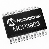
MCP3903-I/SS Microchip Technology, MCP3903-I/SS Datasheet - Page 43

MCP3903-I/SS
Manufacturer Part Number
MCP3903-I/SS
Description
IC AFE 24BIT 64KSPS 28SSOP
Manufacturer
Microchip Technology
Series
-r
Datasheet
1.MCP3903-ISS.pdf
(54 pages)
Specifications of MCP3903-I/SS
Featured Product
MCP3903 Six Channel ÎΣ A/D Converter
Number Of Bits
24
Number Of Channels
6
Power (watts)
-
Voltage - Supply, Analog
4.5 V ~ 5.5 V
Voltage - Supply, Digital
2.7 V ~ 3.6 V
Package / Case
28-SSOP (0.209", 5.30mm Width)
Lead Free Status / Rohs Status
Lead free / RoHS Compliant
Available stocks
Company
Part Number
Manufacturer
Quantity
Price
Company:
Part Number:
MCP3903-I/SS
Manufacturer:
Microchip
Quantity:
263
Part Number:
MCP3903-I/SS
Manufacturer:
MICROCHIP/微芯
Quantity:
20 000
REGISTER 7-5:
© 2011 Microchip Technology Inc.
bit 20:15
bit 14
bit 13
bit 12
bit 11:10
bit 9:8
bit 7:6
bit 5:0
WIDTH_CHn ADC Channels output data word width control
1 = 24-bit mode for the corresponding channel
0 = 16-bit mode for the corresponding channel (default)
DR_LTY: Data Ready Latency Control for DRA, DRB, and DRC pins
1 = True “No Latency” Conversion, data ready pulses after 3 DRCLK periods (DEFAULT)
0 = Unsettled Data is available after every DRCLK period
DR_HIZ: Data Ready Pin Inactive State Control for DRA, DRB, and DRC pins
1 = The Default state is a logic high when data is NOT ready
0 = The Default state is high impedance when data is NOT ready (DEFAULT)
DR_LINK Data Ready Link Control
1 = Data Ready Link turned ON, all channels linked and data ready pulses from the most lagging ADC
0 = Data Ready Link tunred OFF (DEFAULT)
DRC_MODE[1:0]
11 = Both Data Ready pulses from CH4 and CH5 are output on DRC pin.
10 = Data Ready pulses from CH5 are output on DRC pin. Data Ready pulses R from CH4 are not pres-
01 = Data Ready pulses from CH4 are output on DRC pin. Data Ready pulses from CH5 are not present
00 = Data Ready pulses from the lagging ADC channel between the two are output on DRC pin. The
DRB_MODE[1:0]
11 = Both Data Ready pulses from CH2 and CH3 are output on DRB pin.
10 = Data Ready pulses from CH3 are output on DRB pin. Data Ready pulses from CH2 are not present
01 = Data Ready pulses from CH2 are output on DRB pin. Data Ready pulses from CH3 are not present
00 = Data Ready pulses from the lagging ADC channel between the two are output on DRB pin. The
DRA_MODE[1:0]
11 = Both Data Ready pulses from CH0 and CH1 are output on DRA pin.
10 = Data Ready pulses from CH1 are output on DRA pin. Data Ready pulses from CH0 are not present
01 = Data Ready pulses from CH0 are output on DRA pin. Data Ready pulses from CH1 are not present
00 = Data Ready pulses from the lagging ADC channel between the two are output on DRA pin. The
DRSTATUS_CHn: Data Ready Status
1 = Data Not Ready (default)
0 = Data Ready
are present on each DRn pin
ent on the pin.
on the pin.
lagging ADC channel depends on the phase register and on the OSR. (DEFAULT)
on the pin.
on the pin.
lagging ADC channel depends on the phase register and on the OSR. (DEFAULT)
on the pin.
on the pin.
lagging ADC channel depends on the phase register and on the OSR. (DEFAULT)
STATUS/COM REGISTER (CONTINUED)
MCP3903
DS25048B-page 43


