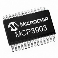
MCP3903-I/SS Microchip Technology, MCP3903-I/SS Datasheet - Page 42

MCP3903-I/SS
Manufacturer Part Number
MCP3903-I/SS
Description
IC AFE 24BIT 64KSPS 28SSOP
Manufacturer
Microchip Technology
Series
-r
Datasheet
1.MCP3903-ISS.pdf
(54 pages)
Specifications of MCP3903-I/SS
Featured Product
MCP3903 Six Channel ÎΣ A/D Converter
Number Of Bits
24
Number Of Channels
6
Power (watts)
-
Voltage - Supply, Analog
4.5 V ~ 5.5 V
Voltage - Supply, Digital
2.7 V ~ 3.6 V
Package / Case
28-SSOP (0.209", 5.30mm Width)
Lead Free Status / Rohs Status
Lead free / RoHS Compliant
Available stocks
Company
Part Number
Manufacturer
Quantity
Price
Company:
Part Number:
MCP3903-I/SS
Manufacturer:
Microchip
Quantity:
263
Part Number:
MCP3903-I/SS
Manufacturer:
MICROCHIP/微芯
Quantity:
20 000
MCP3903
7.5
TABLE 7-7:
7.5.1
This bit determines if the data ready pulses correspond
to settled data or unsettled data from each SINC
Unsettled data will provide data ready pulses every
DRCLK period. Settled data will wait for 3 DRCLK
periods before giving data ready pulses and will then
give data ready pulses every DRCLK period.
7.5.2
Using this bit, the user can connect multiple chips with
the same data ready pin with a pull up resistor
(DR_HIZ=0) or a single chip with no external compo-
nent (DR_HIZ=1)
7.5.3
These bits control which ADC data ready is present on
the data ready pin. When the bits are set to 00, the
output of the two ADCs are latched synchronously at
the moment of the data ready event. This prevents bad
synchronization between the two ADCs. The output is
also latched at the beginning of a reading, in order not
to be updated during a read, and not to give erroneous
data.
REGISTER 7-5:
DS25048B-page 42
bit 23
bit 15
bit 7
bit 23:22
bit 21
DRA_MODE1
WIDTH_CH0
STATUS/COM
READ1
R/W-1
R/W-0
R/W-0
Name
STATUS/COM Register - Status
and Communication Register
DATA READY LATENCY - DR_LTY
DATA READY HIGH Z MODE -
DR_HIZ
DATA READY MODE - DRN_MODE
READ[1:0]: Address Loop Setting
11 = Address counter incremented, cycle through entire register map
10 = Address counter loops on register TYPES (DEFAULT)
01 = Address counter loops on register GROUPS
00 = Address not incremented, continually read single register
WMODE: Write Mode Bit (internal use only)
1 = Static addressing Write Mode
0 = Incremental addressing Write Mode (DEFAULT)
DRA_MODE0 DRSTATUS_CH5 DRSTATUS_CH4 DRSTATUS_CH3 DRSTATUS_CH2 DRSTATUS_CH1 DRSTATUS_CH0
DR_LTY
READ0
R/W-0
R/W-1
R/W-0
STATUS/COM Register
Bits
24
STATUS/COM REGISTER
WMODE
DR_HIZ
R/W-0
R/W-0
R-1
Address
0x09
WIDTH_CH5
DR_LINK
R/W-0
R/W-0
R-1
R/W
3
Cof
filter.
DRC_MODE1
WIDTH_CH4
R/W-0
R/W-0
R-1
If one of the channels is in reset or shutdown, only one
of the data ready pulses is present and the situation is
similar to DRn_MODE<1:0> = 01 or 10. In the 01,10
and 11 modes, the data is latched at the beginning of a
reading, in order to prevent the case of erroneous data
when a data ready pulse happens when reading.
7.5.4
These bits indicate the data ready status of each chan-
nel. These flags are set to logic high after being the
STATUS/COM register has been read. These bits are
cleared when a data ready event has happened on its
respective ADC. Writing these bits has no effect.
Note:
DRC_MODE0
WIDTH_CH3
DATA READY STATUS FLAG -
DRSTATUS_CHN
These bits are useful if multiple devices
share
(DR_HIZ=0) in order to understand which
device the data ready event occured from.
In case the DRn_MODE=00 (Linked
ADCs), these data ready status bits will be
updated synchronously upon the same
event (lagging ADC is ready). These bits
are also useful in systems where the DRn
pins are not used to save MCU I/O.
R/W-0
R/W-0
R-1
the
© 2011 Microchip Technology Inc.
same
DRB_MODE1
WIDTH_CH2
R/W-0
R/W-0
R-1
DRn
output
DRB_MODE0
WIDTH_CH1
R/W-0
R/W-0
R-1
bit 16
pin
bit 8
bit 0


