AT45DB321D-TU Atmel, AT45DB321D-TU Datasheet - Page 10
AT45DB321D-TU
Manufacturer Part Number
AT45DB321D-TU
Description
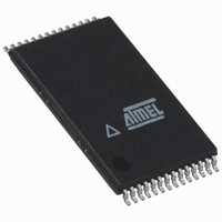
IC FLASH 32MBIT 66MHZ 28TSOP
Manufacturer
Atmel
Specifications of AT45DB321D-TU
Format - Memory
FLASH
Memory Type
DataFLASH
Memory Size
32M (8192 pages x 528 bytes)
Speed
66MHz
Interface
SPI, RapidS
Voltage - Supply
2.7 V ~ 3.6 V
Operating Temperature
-40°C ~ 85°C
Package / Case
28-TSOP
Architecture
Sectored
Interface Type
SPI
Supply Voltage (max)
3.6 V
Supply Voltage (min)
2.7 V
Maximum Operating Current
15 mA
Mounting Style
SMD/SMT
Organization
528 B x 8192
Memory Configuration
8192 Pages X 528 Bytes
Clock Frequency
20MHz
Supply Voltage Range
2.7V To 3.6V
Memory Case Style
TSOP
Rohs Compliant
Yes
Lead Free Status / RoHS Status
Lead free / RoHS Compliant
Available stocks
Company
Part Number
Manufacturer
Quantity
Price

Part Number:
AT45DB321D-TU
Manufacturer:
ATMEL/爱特梅尔
Quantity:
20 000


7.6
Table 7-2.
7.7
10
PA12/
A21
0
0
0
0
1
1
1
1
•
•
•
Sector Erase
Chip Erase
PA11/
AT45DB321D
A20
0
0
0
0
1
1
1
1
•
•
•
Sector Erase Addressing
PA10/
A19
0
0
0
0
1
1
1
1
•
•
•
(1)
The Sector Erase command can be used to individually erase any sector in the main memory.
There are 64 sectors and only one sector can be erased at one time. To perform sector 0a or
sector 0b erase for the DataFlash standard page size (528 bytes), an opcode of 7CH must be
loaded into the device, followed by three address bytes comprised of 1 don’t care bit, 10 page
address bits (PA12 - PA3) and 13 don’t care bits. To perform a sector 1-63 erase, the opcode
7CH must be loaded into the device, followed by three address bytes comprised of 1 don’t
care bit, 6 page address bits (PA12 - PA7) and 17 don’t care bits. To perform sector 0a or sector
0b erase for the binary page size (512 bytes), an opcode of 7CH must be loaded into the
device, followed by three address bytes comprised of 2 don’t care bit and 10 page address bits
(A21 - A12) and 12 don’t care bits. To perform a sector 1-63 erase, the opcode 7CH must be
loaded into the device, followed by three address bytes comprised of 2 don’t care bits and
6 page address bits (A21 - A16) and 16 don’t care bits. The page address bits are used to spec-
ify any valid address location within the sector which is to be erased. When a low-to-high
transition occurs on the CS pin, the part will erase the selected sector. The erase operation is
internally self-timed and should take place in a maximum time of t
register and the RDY/BUSY pin will indicate that the part is busy.
The entire main memory can be erased at one time by using the Chip Erase command.
To execute the Chip Erase command, a 4-byte command sequence C7H, 94H, 80H and 9AH
must be clocked into the device. Since the entire memory array is to be erased, no address
bytes need to be clocked into the device, and any data clocked in after the opcode will be
ignored. After the last bit of the opcode sequence has been clocked in, the CS pin can be deas-
serted to start the erase process. The erase operation is internally self-timed and should take
place in a time of t
The Chip Erase command will not affect sectors that are protected or locked down; the contents
of those sectors will remain unchanged. Only those sectors that are not protected or locked
down will be erased.
Note:
PA9/
A18
0
0
0
0
1
1
1
1
•
•
•
1. Refer to the errata regarding Chip Erase on
PA8/
A17
0
0
0
1
0
0
1
1
•
•
•
PA7/
A16
CE
0
0
1
0
0
1
0
1
•
•
•
. During this time, the Status Register will indicate that the device is busy.
PA6/
A15
X
X
X
X
X
X
0
0
•
•
•
PA5/
A14
X
X
X
X
X
X
0
0
•
•
•
PA4/
A13
X
X
X
X
X
X
0
0
•
•
•
page
PA3/
A12
X
X
X
X
X
X
0
1
•
•
•
56.
PA2/
A11
X
X
X
X
X
X
X
X
•
•
•
SE
. During this time, the status
PA1/
A10
X
X
X
X
X
X
X
X
•
•
•
PA0/
A9
X
X
X
X
X
X
X
X
•
•
•
3597O–DFLASH–10/09
Sector
0a
0b
60
61
62
63
1
2
•
•
•
Related parts for AT45DB321D-TU
Image
Part Number
Description
Manufacturer
Datasheet
Request
R

Part Number:
Description:
DEV KIT FOR AVR/AVR32
Manufacturer:
Atmel
Datasheet:

Part Number:
Description:
INTERVAL AND WIPE/WASH WIPER CONTROL IC WITH DELAY
Manufacturer:
ATMEL Corporation
Datasheet:
Part Number:
Description:
Low-Voltage Voice-Switched IC for Hands-Free Operation
Manufacturer:
ATMEL Corporation
Datasheet:
Part Number:
Description:
MONOLITHIC INTEGRATED FEATUREPHONE CIRCUIT
Manufacturer:
ATMEL Corporation
Datasheet:
Part Number:
Description:
AM-FM Receiver IC U4255BM-M
Manufacturer:
ATMEL Corporation
Datasheet:
Part Number:
Description:
Monolithic Integrated Feature Phone Circuit
Manufacturer:
ATMEL Corporation
Datasheet:
Part Number:
Description:
Multistandard Video-IF and Quasi Parallel Sound Processing
Manufacturer:
ATMEL Corporation
Datasheet:
Part Number:
Description:
High-performance EE PLD
Manufacturer:
ATMEL Corporation
Datasheet:
Part Number:
Description:
8-bit Flash Microcontroller
Manufacturer:
ATMEL Corporation
Datasheet:
Part Number:
Description:
2-Wire Serial EEPROM
Manufacturer:
ATMEL Corporation
Datasheet: