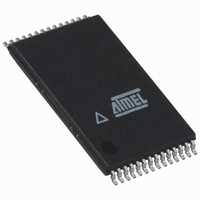
AT45DB321D-TU Atmel, AT45DB321D-TU Datasheet - Page 15

AT45DB321D-TU
Manufacturer Part Number
AT45DB321D-TU
Description
IC FLASH 32MBIT 66MHZ 28TSOP
Manufacturer
Atmel
Specifications of AT45DB321D-TU
Format - Memory
FLASH
Memory Type
DataFLASH
Memory Size
32M (8192 pages x 528 bytes)
Speed
66MHz
Interface
SPI, RapidS
Voltage - Supply
2.7 V ~ 3.6 V
Operating Temperature
-40°C ~ 85°C
Package / Case
28-TSOP
Architecture
Sectored
Interface Type
SPI
Supply Voltage (max)
3.6 V
Supply Voltage (min)
2.7 V
Maximum Operating Current
15 mA
Mounting Style
SMD/SMT
Organization
528 B x 8192
Memory Configuration
8192 Pages X 528 Bytes
Clock Frequency
20MHz
Supply Voltage Range
2.7V To 3.6V
Memory Case Style
TSOP
Rohs Compliant
Yes
Lead Free Status / RoHS Status
Lead free / RoHS Compliant
Available stocks
Company
Part Number
Manufacturer
Quantity
Price
Part Number:
AT45DB321D-TU
Manufacturer:
ATMEL/爱特梅尔
Quantity:
20 000
9.1.1
9.1.2
3597O–DFLASH–10/09
Erase Sector Protection Register Command
Program Sector Protection Register Command
In order to modify and change the values of the Sector Protection Register, it must first be
erased using the Erase Sector Protection Register command.
To erase the Sector Protection Register, the CS pin must first be asserted as it would be with
any other command. Once the CS pin has been asserted, the appropriate 4-byte opcode
sequence must be clocked into the device via the SI pin. The 4-byte opcode sequence must
start with 3DH and be followed by 2AH, 7FH, and CFH. After the last bit of the opcode sequence
has been clocked in, the CS pin must be deasserted to initiate the internally self-timed erase
cycle. The erasing of the Sector Protection Register should take place in a time of t
which time the Status Register will indicate that the device is busy. If the device is powered-
down before the completion of the erase cycle, then the contents of the Sector Protection Regis-
ter cannot be guaranteed.
The Sector Protection Register can be erased with the sector protection enabled or disabled.
Since the erased state (FFH) of each byte in the Sector Protection Register is used to indicate
that a sector is specified for protection, leaving the sector protection enabled during the erasing
of the register allows the protection scheme to be more effective in the prevention of accidental
programming or erasing of the device. If for some reason an erroneous program or erase com-
mand is sent to the device immediately after erasing the Sector Protection Register and before
the register can be reprogrammed, then the erroneous program or erase command will not be
processed because all sectors would be protected.
Figure 9-2.
Once the Sector Protection Register has been erased, it can be reprogrammed using the Pro-
gram Sector Protection Register command.
To program the Sector Protection Register, the CS pin must first be asserted and the appropri-
ate 4-byte opcode sequence must be clocked into the device via the SI pin. The 4-byte opcode
sequence must start with 3DH and be followed by 2AH, 7FH, and FCH. After the last bit of the
opcode sequence has been clocked into the device, the data for the contents of the Sector Pro-
tection Register must be clocked in. As described in
contains 64 bytes of data, so 64 bytes must be clocked into the device. The first byte of data cor-
responds to sector 0, the second byte corresponds to sector 1, and so on with the last byte of
data corresponding to sector 63.
Command
Erase Sector Protection Register
Erase Sector Protection Register
CS
SI
Each transition
represents 8 bits
Opcode
Byte 1
Byte 1
Opcode
Byte 2
3DH
Section
Opcode
Byte 3
Byte 2
2AH
9.1, the Sector Protection Register
Opcode
Byte 4
AT45DB321D
Byte 3
7FH
Byte 4
PE
CFH
, during
15


