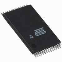
AT45DB321D-TU Atmel, AT45DB321D-TU Datasheet - Page 21

AT45DB321D-TU
Manufacturer Part Number
AT45DB321D-TU
Description
IC FLASH 32MBIT 66MHZ 28TSOP
Manufacturer
Atmel
Specifications of AT45DB321D-TU
Format - Memory
FLASH
Memory Type
DataFLASH
Memory Size
32M (8192 pages x 528 bytes)
Speed
66MHz
Interface
SPI, RapidS
Voltage - Supply
2.7 V ~ 3.6 V
Operating Temperature
-40°C ~ 85°C
Package / Case
28-TSOP
Architecture
Sectored
Interface Type
SPI
Supply Voltage (max)
3.6 V
Supply Voltage (min)
2.7 V
Maximum Operating Current
15 mA
Mounting Style
SMD/SMT
Organization
528 B x 8192
Memory Configuration
8192 Pages X 528 Bytes
Clock Frequency
20MHz
Supply Voltage Range
2.7V To 3.6V
Memory Case Style
TSOP
Rohs Compliant
Yes
Lead Free Status / RoHS Status
Lead free / RoHS Compliant
Available stocks
Company
Part Number
Manufacturer
Quantity
Price
Part Number:
AT45DB321D-TU
Manufacturer:
ATMEL/爱特梅尔
Quantity:
20 000
10.2.2
Figure 10-4. Read Security Register
11. Additional Commands
11.1
3597O–DFLASH–10/09
Main Memory Page to Buffer Transfer
CS
SO
Reading the Security Register
SI
Each transition
represents 8 bits
Opcode
The Security Register can be read by first asserting the CS pin and then clocking in an opcode
of 77H followed by three dummy bytes. After the last don't care bit has been clocked in, the con-
tent of the Security Register can be clocked out on the SO pins. After the last byte of the
Security Register has been read, additional pulses on the SCK pin will simply result in undefined
data being output on the SO pins.
Deasserting the CS pin will terminate the Read Security Register operation and put the SO pins
into a high-impedance state.
A page of data can be transferred from the main memory to either buffer 1 or buffer 2. To start
the operation for the DataFlash standard page size (528 bytes), a 1-byte opcode, 53H for buffer
1 and 55H for buffer 2, must be clocked into the device, followed by three address bytes com-
prised of 1 don’t care bit, 13-page address bit (PA12 - PA0), which specify the page in main
memory that is to be transferred, and 10 don’t care bits. To perform a main memory page to buf-
fer transfer for the binary page size (512 bytes), the opcode 53H for buffer 1 or 55H for buffer 2,
must be clocked into the device followed by three address bytes consisting of 2 don’t care bits,
13-page address bits (A21 - A9) which specify the page in the main memory that is to be trans-
ferred, and 9 don’t care bits. The CS pin must be low while toggling the SCK pin to load the
opcode and the address bytes from the input pin (SI). The transfer of the page of data from the
main memory to the buffer will begin when the CS pin transitions from a low to a high state. Dur-
ing the transfer of a page of data (t
monitored to determine whether the transfer has been completed.
X
X
XFR
X
), the status register can be read or the RDY/BUSY can be
Data Byte
n
Data Byte
n + 1
AT45DB321D
Data Byte
n + x
21


