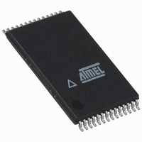
AT45DB321D-TU Atmel, AT45DB321D-TU Datasheet - Page 22

AT45DB321D-TU
Manufacturer Part Number
AT45DB321D-TU
Description
IC FLASH 32MBIT 66MHZ 28TSOP
Manufacturer
Atmel
Specifications of AT45DB321D-TU
Format - Memory
FLASH
Memory Type
DataFLASH
Memory Size
32M (8192 pages x 528 bytes)
Speed
66MHz
Interface
SPI, RapidS
Voltage - Supply
2.7 V ~ 3.6 V
Operating Temperature
-40°C ~ 85°C
Package / Case
28-TSOP
Architecture
Sectored
Interface Type
SPI
Supply Voltage (max)
3.6 V
Supply Voltage (min)
2.7 V
Maximum Operating Current
15 mA
Mounting Style
SMD/SMT
Organization
528 B x 8192
Memory Configuration
8192 Pages X 528 Bytes
Clock Frequency
20MHz
Supply Voltage Range
2.7V To 3.6V
Memory Case Style
TSOP
Rohs Compliant
Yes
Lead Free Status / RoHS Status
Lead free / RoHS Compliant
Available stocks
Company
Part Number
Manufacturer
Quantity
Price
Part Number:
AT45DB321D-TU
Manufacturer:
ATMEL/爱特梅尔
Quantity:
20 000
11.2
11.3
22
Main Memory Page to Buffer Compare
Auto Page Rewrite
AT45DB321D
A page of data in the main memory can be compared to the data in buffer 1 or buffer 2. To initi-
ate the operation for DataFlash standard page size, a 1-byte opcode, 60H for buffer 1 and 61H
for buffer 2, must be clocked into the device, followed by three address bytes consisting of
1 don’t care bit, 13-page address bits (PA12 - PA0) that specify the page in the main memory
that is to be compared to the buffer, and 10 don’t care bits. To start a main memory page to buf-
fer compare for a binary page size, the opcode 60H for buffer 1 or 61H for buffer 2, must be
clocked into the device followed by three address bytes consisting of 2 don’t care bits, 13 page
address bits (A21 - A9) that specify the page in the main memory that is to be compared to the
buffer, and 9 don’t care bits. The CS pin must be low while toggling the SCK pin to load the
opcode and the address bytes from the input pin (SI). On the low-to-high transition of the CS pin,
the data bytes in the selected main memory page will be compared with the data bytes in buffer
1 or buffer 2. During this time (t
the part is busy. On completion of the compare operation, bit 6 of the status register is updated
with the result of the compare.
This mode is only needed if multiple bytes within a page or multiple pages of data are modified in
a random fashion within a sector. This mode is a combination of two operations: Main Memory
Page to Buffer Transfer and Buffer to Main Memory Page Program with Built-in Erase. A page of
data is first transferred from the main memory to buffer 1 or buffer 2, and then the same data
(from buffer 1 or buffer 2) is programmed back into its original page of main memory. To start the
rewrite operation for the DataFlash standard page size (528 bytes), a 1-byte opcode, 58H for
buffer 1 or 59H for buffer 2, must be clocked into the device, followed by three address bytes
comprised of 1 don’t care bit, 13-page address bits (PA12-PA0) that specify the page in main
memory to be rewritten and 10 don’t care bits. To initiate an auto page rewrite for a binary page
size (512 bytes), the opcode 58H for buffer 1 or 59H for buffer 2, must be clocked into the device
followed by three address bytes consisting of 2 don’t care bits, 13 page address bits (A21 - A9)
that specify the page in the main memory that is to be written and 9 don’t care bits. When a low-
to-high transition occurs on the CS pin, the part will first transfer data from the page in main
memory to a buffer and then program the data from the buffer back into same page of main
memory. The operation is internally self-timed and should take place in a maximum time of t
During this time, the status register and the RDY/BUSY pin will indicate that the part is busy.
If a sector is programmed or reprogrammed sequentially page by page, then the programming
algorithm shown in
page or several pages are programmed randomly in a sector, then the programming algorithm
shown in
updated/rewritten at least once within every 10,000 cumulative page erase/program operations
in that sector.
Figure 25-2 (page
Figure 25-1 (page
COMP
47) is recommended. Each page within a sector must be
), the status register and the RDY/BUSY pin will indicate that
46) is recommended. Otherwise, if multiple bytes in a
3597O–DFLASH–10/09
EP
.


