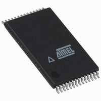
AT45DB321D-TU Atmel, AT45DB321D-TU Datasheet - Page 8

AT45DB321D-TU
Manufacturer Part Number
AT45DB321D-TU
Description
IC FLASH 32MBIT 66MHZ 28TSOP
Manufacturer
Atmel
Specifications of AT45DB321D-TU
Format - Memory
FLASH
Memory Type
DataFLASH
Memory Size
32M (8192 pages x 528 bytes)
Speed
66MHz
Interface
SPI, RapidS
Voltage - Supply
2.7 V ~ 3.6 V
Operating Temperature
-40°C ~ 85°C
Package / Case
28-TSOP
Architecture
Sectored
Interface Type
SPI
Supply Voltage (max)
3.6 V
Supply Voltage (min)
2.7 V
Maximum Operating Current
15 mA
Mounting Style
SMD/SMT
Organization
528 B x 8192
Memory Configuration
8192 Pages X 528 Bytes
Clock Frequency
20MHz
Supply Voltage Range
2.7V To 3.6V
Memory Case Style
TSOP
Rohs Compliant
Yes
Lead Free Status / RoHS Status
Lead free / RoHS Compliant
Available stocks
Company
Part Number
Manufacturer
Quantity
Price
Part Number:
AT45DB321D-TU
Manufacturer:
ATMEL/爱特梅尔
Quantity:
20 000
7. Program and Erase Commands
7.1
7.2
7.3
8
Buffer Write
Buffer to Main Memory Page Program with Built-in Erase
Buffer to Main Memory Page Program without Built-in Erase
AT45DB321D
Data can be clocked in from the input pin (SI) into either buffer 1 or buffer 2. To load data into the
DataFlash standard buffer (528 bytes), a 1-byte opcode, 84H for buffer 1 or 87H for buffer 2,
must be clocked into the device, followed by three address bytes comprised of 14 don’t care bits
and 10 buffer address bits (BFA9 - BFA0). The 10 buffer address bits specify the first byte in the
buffer to be written. To load data into the binary buffers (512 bytes each), a 1-byte opcode 84H
for buffer 1 or 87H for buffer 2, must be clocked into the device, followed by three address bytes
comprised of 15 don’t care bits and 9 buffer address bits (BFA8 - BFA0). The 9 buffer address
bits specify the first byte in the buffer to be written. After the last address byte has been clocked
into the device, data can then be clocked in on subsequent clock cycles. If the end of the data
buffer is reached, the device will wrap around back to the beginning of the buffer. Data will con-
tinue to be loaded into the buffer until a low-to-high transition is detected on the CS pin.
Data written into either buffer 1 or buffer 2 can be programmed into the main memory. A 1-byte
opcode, 83H for buffer 1 or 86H for buffer 2, must be clocked into the device. For the DataFlash
standard page size (528 bytes), the opcode must be followed by three address bytes consist of
1 don’t care bit, 13 page address bits (PA12 - PA0) that specify the page in the main memory to
be written and 10 don’t care bits. To perform a buffer to main memory page program with built-in
erase for the binary page size (512 bytes), the opcode 83H for buffer 1 or 86H for buffer 2, must
be clocked into the device followed by three address bytes consisting of 2 don’t care bits
13-page address bits (A21 - A9) that specify the page in the main memory to be written and
9 don’t care bits. When a low-to-high transition occurs on the CS pin, the part will first erase the
selected page in main memory (the erased state is a logic 1) and then program the data stored
in the buffer into the specified page in main memory. Both the erase and the programming of the
page are internally self-timed and should take place in a maximum time of t
the status register and the RDY/BUSY pin will indicate that the part is busy.
A previously-erased page within main memory can be programmed with the contents of either
buffer 1 or buffer 2. A 1-byte opcode, 88H for buffer 1 or 89H for buffer 2, must be clocked into
the device. For the DataFlash standard page size (528 bytes), the opcode must be followed by
three address bytes consist of 1 don’t care bit, 13 page address bits (PA12 - PA0) that specify
the page in the main memory to be written and 10 don’t care bits. To perform a buffer to main
memory page program without built-in erase for the binary page size (512 bytes), the opcode
88H for buffer 1 or 89H for buffer 2, must be clocked into the device followed by three address
bytes consisting of 2 don’t care bits, 13 page address bits (A21 - A9) that specify the page in the
main memory to be written and 9 don’t care bits. When a low-to-high transition occurs on the CS
pin, the part will program the data stored in the buffer into the specified page in the main mem-
ory. It is necessary that the page in main memory that is being programmed has been previously
erased using one of the erase commands (Page Erase or Block Erase). The programming of the
page is internally self-timed and should take place in a maximum time of t
status register and the RDY/BUSY pin will indicate that the part is busy.
P
. During this time, the
EP
. During this time,
3597O–DFLASH–10/09


