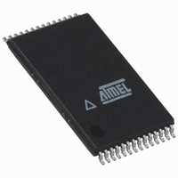
AT45DB321D-TU Atmel, AT45DB321D-TU Datasheet - Page 5

AT45DB321D-TU
Manufacturer Part Number
AT45DB321D-TU
Description
IC FLASH 32MBIT 66MHZ 28TSOP
Manufacturer
Atmel
Specifications of AT45DB321D-TU
Format - Memory
FLASH
Memory Type
DataFLASH
Memory Size
32M (8192 pages x 528 bytes)
Speed
66MHz
Interface
SPI, RapidS
Voltage - Supply
2.7 V ~ 3.6 V
Operating Temperature
-40°C ~ 85°C
Package / Case
28-TSOP
Architecture
Sectored
Interface Type
SPI
Supply Voltage (max)
3.6 V
Supply Voltage (min)
2.7 V
Maximum Operating Current
15 mA
Mounting Style
SMD/SMT
Organization
528 B x 8192
Memory Configuration
8192 Pages X 528 Bytes
Clock Frequency
20MHz
Supply Voltage Range
2.7V To 3.6V
Memory Case Style
TSOP
Rohs Compliant
Yes
Lead Free Status / RoHS Status
Lead free / RoHS Compliant
Available stocks
Company
Part Number
Manufacturer
Quantity
Price
Part Number:
AT45DB321D-TU
Manufacturer:
ATMEL/爱特梅尔
Quantity:
20 000
5. Device Operation
6. Read Commands
6.1
3597O–DFLASH–10/09
Continuous Array Read (Legacy Command: E8H): Up to 66 MHz
The device operation is controlled by instructions from the host processor. The list of instructions
and their associated opcodes are contained in
page
opcode and the desired buffer or main memory address location. While the CS pin is low, tog-
gling the SCK pin controls the loading of the opcode and the desired buffer or main memory
address location through the SI (serial input) pin. All instructions, addresses, and data are trans-
ferred with the most significant bit (MSB) first.
Buffer addressing for the DataFlash standard page size (528 bytes) is referenced in the
datasheet using the terminology BFA9 - BFA0 to denote the 10 address bits required to desig-
nate a byte address within a buffer. Main memory addressing is referenced using the
terminology PA12 - PA0 and BA9 - BA0, where PA12 - PA0 denotes the 13 address bits
required to designate a page address and BA9 - BA0 denotes the 10 address bits required to
designate a byte address within the page.
For “Power of 2” binary page size (512 bytes) the Buffer addressing is referenced in the
datasheet using the conventional terminology BFA8 - BFA0 to denote the 9 address bits
required to designate a byte address within a buffer. Main memory addressing is referenced
using the terminology A21 - A0, where A21 - A9 denotes the 13 address bits required to desig-
nate a page address and A8 - A0 denotes the 9 address bits required to designate a byte
address within a page.
By specifying the appropriate opcode, data can be read from the main memory or from either
one of the two SRAM data buffers. The DataFlash supports RapidS protocols for Mode 0 and
Mode 3. Please refer to the “Detailed Bit-level Read Timing” diagrams in this datasheet for
details on the clock cycle sequences for each mode.
By supplying an initial starting address for the main memory array, the Continuous Array Read
command can be utilized to sequentially read a continuous stream of data from the device by
simply providing a clock signal; no additional addressing information or control signals need to
be provided. The DataFlash incorporates an internal address counter that will automatically
increment on every clock cycle, allowing one continuous read operation without the need of
additional address sequences. To perform a continuous read from the DataFlash standard page
size (528 bytes), an opcode of E8H must be clocked into the device followed by three address
bytes (which comprise the 24-bit page and byte address sequence) and 4 don’t care bytes. The
first 13 bits (PA12 - PA0) of the 23-bit address sequence specify which page of the main mem-
ory array to read, and the last 10 bits (BA9 - BA0) of the 23-bit address sequence specify the
starting byte address within the page. To perform a continuous read from the binary page size
(512 bytes), the opcode (E8H) must be clocked into the device followed by three address bytes
and 4 don’t care bytes. The first 13 bits (A21 - A9) of the 22-bits sequence specify which page of
the main memory array to read, and the last 9 bits (A8 - A0) of the 22-bits address sequence
specify the starting byte address within the page. The don’t care bytes that follow the address
bytes are needed to initialize the read operation. Following the don’t care bytes, additional clock
pulses on the SCK pin will result in data being output on the SO (serial output) pin.
The CS pin must remain low during the loading of the opcode, the address bytes, the don’t care
bytes, and the reading of data. When the end of a page in main memory is reached during a
31. A valid instruction starts with the falling edge of CS followed by the appropriate 8-bit
Table 15-1 on page 28
AT45DB321D
through
Table 15-7 on
5


