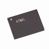
AT45DB642D-CNU Atmel, AT45DB642D-CNU Datasheet - Page 10

AT45DB642D-CNU
Manufacturer Part Number
AT45DB642D-CNU
Description
IC FLASH 64MBIT 66MHZ 8CASON
Manufacturer
Atmel
Datasheet
1.AT45DB642D-CU.pdf
(58 pages)
Specifications of AT45DB642D-CNU
Format - Memory
FLASH
Memory Type
DataFLASH
Memory Size
64M (8192 pages x 1056 bytes)
Speed
66MHz
Interface
Parallel/Serial
Voltage - Supply
2.7 V ~ 3.6 V
Operating Temperature
-40°C ~ 85°C
Package / Case
8-CASON
Package
8CASON
Density
64 Mb
Architecture
Sectored
Block Organization
Symmetrical
Typical Operating Supply Voltage
3.3 V
Sector Size
256KByte x 32
Timing Type
Synchronous
Interface Type
Parallel|Serial-SPI
Data Bus Width
8 bit
Supply Voltage (max)
3.6 V
Supply Voltage (min)
2.7 V
Maximum Operating Current
15 mA
Mounting Style
SMD/SMT
Organization
256 KB x 32
Ic Interface Type
Parallel, Serial
Clock Frequency
66MHz
Supply Voltage Range
2.7V To 3.6V
No. Of Pins
8
Operating Temperature Range
-40°C To +85°C
Rohs Compliant
Yes
Lead Free Status / RoHS Status
Lead free / RoHS Compliant
Available stocks
Company
Part Number
Manufacturer
Quantity
Price
Company:
Part Number:
AT45DB642D-CNU
Manufacturer:
MICRON
Quantity:
1 001
Company:
Part Number:
AT45DB642D-CNU
Manufacturer:
Atmel
Quantity:
59
Company:
Part Number:
AT45DB642D-CNU
Manufacturer:
AMTEL
Quantity:
143
Part Number:
AT45DB642D-CNU
Manufacturer:
ATMEL/爱特梅尔
Quantity:
20 000
Company:
Part Number:
AT45DB642D-CNU SL954
Manufacturer:
ATMEL
Quantity:
200
Part Number:
AT45DB642D-CNU SL954
Manufacturer:
ATMEL/爱特梅尔
Quantity:
20 000
Company:
Part Number:
AT45DB642D-CNU-SL954
Manufacturer:
PAM
Quantity:
34 000
7.4
7.5
Table 7-1.
10
PA12/
A22
0
0
0
0
1
1
1
1
•
•
•
Page Erase
Block Erase
AT45DB642D
PA11/
A21
0
0
0
0
1
1
1
1
•
•
•
Block Erase Addressing
PA10/
A20
0
0
0
0
1
1
1
1
•
•
•
page in main memory that is being programmed has been previously erased using one of the
erase commands (Page Erase or Block Erase). The programming of the page is internally self-
timed and should take place in a maximum time of t
the RDY/BUSY pin will indicate that the part is busy.
The Page Erase command can be used to individually erase any page in the main memory array
allowing the Buffer to Main Memory Page Program to be utilized at a later time. To perform a
page erase in the standard DataFlash page size (1056 bytes), an opcode of 81H must be loaded
into the device, followed by three address bytes comprised of 13 page address bits (PA12 -
a page erase in the binary page size (1024 bytes), the opcode 81H must be loaded into the
device, followed by three address bytes consist of 13 page address bits (A22 - A10) that specify
the page in the main memory to be erased and 10 don’t care bits. When a low-to-high transition
occurs on the CS pin, the part will erase the selected page (the erased state is a logical 1). The
erase operation is internally self-timed and should take place in a maximum time of t
this time, the status register and the RDY/BUSY pin will indicate that the part is busy.
A block of eight pages can be erased at one time. This command is useful when large amounts
of data has to be written into the device. This will avoid using multiple Page Erase Commands.
To perform a block erase for the standard DataFlash page size (1056 bytes), an opcode of 50H
must be loaded into the device, followed by three address bytes comprised of 10 page address
bits (PA12 -PA3) and 14 don’t care bits. The 10 page address bits are used to specify which
block of eight pages is to be erased. To perform a block erase for the binary page size (1024
bytes), the opcode 50H must be loaded into the device, followed by three address bytes consist-
ing of 10 page address bits (A22 - A13) and 13 don’t care bits. The 10 page address bits are
used to specify which block of eight pages is to be erased. When a low-to-high transition occurs
on the CS pin, the part will erase the selected block of eight pages. The erase operation is inter-
nally self-timed and should take place in a maximum time of t
register and the RDY/BUSY pin will indicate that the part is busy.
PA0) that specify the page in the main memory to be erased and 11 don’t care bits. To perform
PA9/
A19
0
0
0
0
1
1
1
1
•
•
•
PA8/
A18
0
0
0
0
1
1
1
1
•
•
•
PA7/
A17
0
0
0
0
1
1
1
1
•
•
•
PA6/
A16
0
0
0
0
1
1
1
1
•
•
•
PA5/
A15
0
0
0
0
1
1
1
1
•
•
•
PA4/
A14
0
0
1
1
0
0
1
1
•
•
•
P
PA3/
A13
. During this time, the status register and
0
1
0
1
0
1
0
1
•
•
•
PA2/
A12
X
X
X
X
X
X
X
X
•
•
•
BE
. During this time, the status
PA1/
A11
X
X
X
X
X
X
X
X
•
•
•
3542K–DFLASH–04/09
PA0/
A10
X
X
X
X
X
X
X
X
•
•
•
PE
. During
Block
1020
1021
1022
1023
0
1
2
3
•
•
•


