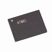
AT45DB642D-CNU Atmel, AT45DB642D-CNU Datasheet - Page 21

AT45DB642D-CNU
Manufacturer Part Number
AT45DB642D-CNU
Description
IC FLASH 64MBIT 66MHZ 8CASON
Manufacturer
Atmel
Datasheet
1.AT45DB642D-CU.pdf
(58 pages)
Specifications of AT45DB642D-CNU
Format - Memory
FLASH
Memory Type
DataFLASH
Memory Size
64M (8192 pages x 1056 bytes)
Speed
66MHz
Interface
Parallel/Serial
Voltage - Supply
2.7 V ~ 3.6 V
Operating Temperature
-40°C ~ 85°C
Package / Case
8-CASON
Package
8CASON
Density
64 Mb
Architecture
Sectored
Block Organization
Symmetrical
Typical Operating Supply Voltage
3.3 V
Sector Size
256KByte x 32
Timing Type
Synchronous
Interface Type
Parallel|Serial-SPI
Data Bus Width
8 bit
Supply Voltage (max)
3.6 V
Supply Voltage (min)
2.7 V
Maximum Operating Current
15 mA
Mounting Style
SMD/SMT
Organization
256 KB x 32
Ic Interface Type
Parallel, Serial
Clock Frequency
66MHz
Supply Voltage Range
2.7V To 3.6V
No. Of Pins
8
Operating Temperature Range
-40°C To +85°C
Rohs Compliant
Yes
Lead Free Status / RoHS Status
Lead free / RoHS Compliant
Available stocks
Company
Part Number
Manufacturer
Quantity
Price
Company:
Part Number:
AT45DB642D-CNU
Manufacturer:
MICRON
Quantity:
1 001
Company:
Part Number:
AT45DB642D-CNU
Manufacturer:
Atmel
Quantity:
59
Company:
Part Number:
AT45DB642D-CNU
Manufacturer:
AMTEL
Quantity:
143
Part Number:
AT45DB642D-CNU
Manufacturer:
ATMEL/爱特梅尔
Quantity:
20 000
Company:
Part Number:
AT45DB642D-CNU SL954
Manufacturer:
ATMEL
Quantity:
200
Part Number:
AT45DB642D-CNU SL954
Manufacturer:
ATMEL/爱特梅尔
Quantity:
20 000
Company:
Part Number:
AT45DB642D-CNU-SL954
Manufacturer:
PAM
Quantity:
34 000
Figure 10-3. Program Security Register
10.2.2
Figure 10-4. Read Security Register
3542K–DFLASH–04/09
SO or IO
SI or IO
SI or IO
Reading the Security Register
7
7
- IO
- IO
CS
7
- IO
CS
0
0
0
Each transition
represents 8 bits
Each transition
represents 8 bits
The Security Register can be read by first asserting the CS pin and then clocking in an opcode
of 77H followed by three dummy bytes if using the serial interface and seven dummy bytes if
using the 8-bit interface. After the last don't care bit has been clocked in, the content of the
Security Register can be clocked out on the SO or I/O7 - I/O0 pins. After the last byte of the
Security Register has been read, additional pulses on the SCK/CLK pin will simply result in
undefined data being output on the SO or I/O7 - I/O0 pins.
Deasserting the CS pin will terminate the Read Security Register operation and put the SO or
I/O7 - I/O0 pins into a high-impedance state.
Opcode
Opcode
Byte 1
Opcode
Byte 2
X
Opcode
Byte 3
X
Opcode
Byte 4
X
Data Byte
n
Data Byte
n
Data Byte
n + 1
Data Byte
n + 1
Data Byte
n + x
Data Byte
n + x
21


