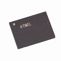
AT45DB642D-CNU Atmel, AT45DB642D-CNU Datasheet - Page 40

AT45DB642D-CNU
Manufacturer Part Number
AT45DB642D-CNU
Description
IC FLASH 64MBIT 66MHZ 8CASON
Manufacturer
Atmel
Datasheet
1.AT45DB642D-CU.pdf
(58 pages)
Specifications of AT45DB642D-CNU
Format - Memory
FLASH
Memory Type
DataFLASH
Memory Size
64M (8192 pages x 1056 bytes)
Speed
66MHz
Interface
Parallel/Serial
Voltage - Supply
2.7 V ~ 3.6 V
Operating Temperature
-40°C ~ 85°C
Package / Case
8-CASON
Package
8CASON
Density
64 Mb
Architecture
Sectored
Block Organization
Symmetrical
Typical Operating Supply Voltage
3.3 V
Sector Size
256KByte x 32
Timing Type
Synchronous
Interface Type
Parallel|Serial-SPI
Data Bus Width
8 bit
Supply Voltage (max)
3.6 V
Supply Voltage (min)
2.7 V
Maximum Operating Current
15 mA
Mounting Style
SMD/SMT
Organization
256 KB x 32
Ic Interface Type
Parallel, Serial
Clock Frequency
66MHz
Supply Voltage Range
2.7V To 3.6V
No. Of Pins
8
Operating Temperature Range
-40°C To +85°C
Rohs Compliant
Yes
Lead Free Status / RoHS Status
Lead free / RoHS Compliant
Available stocks
Company
Part Number
Manufacturer
Quantity
Price
Company:
Part Number:
AT45DB642D-CNU
Manufacturer:
MICRON
Quantity:
1 001
Company:
Part Number:
AT45DB642D-CNU
Manufacturer:
Atmel
Quantity:
59
Company:
Part Number:
AT45DB642D-CNU
Manufacturer:
AMTEL
Quantity:
143
Part Number:
AT45DB642D-CNU
Manufacturer:
ATMEL/爱特梅尔
Quantity:
20 000
Company:
Part Number:
AT45DB642D-CNU SL954
Manufacturer:
ATMEL
Quantity:
200
Part Number:
AT45DB642D-CNU SL954
Manufacturer:
ATMEL/爱特梅尔
Quantity:
20 000
Company:
Part Number:
AT45DB642D-CNU-SL954
Manufacturer:
PAM
Quantity:
34 000
21.8
Figure 21-2. Rapid8 Mode
21.9
Note:
40
MOSI = Master Out, Slave In
MISO = Master In, Slave Out
The Master would be the ASIC/MCU and the Slave would be the memory device.
The Master always clocks data out on the rising edge of SCK and always clocks data in on the falling edge of SCK.
The Slave always clocks data out on the falling edge of SCK and always clocks data in on the rising edge of SCK.
Slave
Utilizing the Rapid8
Reset Timing
The CS signal should be in the high state before the RESET signal is deasserted.
A.
B.
C.
D.
E.
F.
G. Master clocks in BYTE h (last output byte).
SO or I/O7 - I/O0
AT45DB642D
SI or I/O7 - I/O0
I/O
SCK
Master clocks out BYTE 1 on the rising edge of SCK.
Slave clocks in BYTE 1 on the next rising edge of SCK.
Master clocks out BYTE 2 on the same rising edge of SCK.
Slave clocks in BYTE 6 (last input byte).
Slave clocks out BYTE a (first output byte).
Master clocks in BYTE a.
CS
7-0
(OUTPUT)
SCK/CLK
(INPUT)
RESET
CS
A
The Rapid8 functions like RapidS but with 8 bits of data instead of 1 bit. A full clock cycle must
be used to transmit data back and forth across the 8 bit bus. The DataFlash is designed to
always clock its data out on the falling edge of the SCK signal and clock data in on the rising
edge of SCK.
For full clock cycle operation to be achieved, when the DataFlash is clocking data out on the fall-
ing edge of SCK, the host controller should wait until the next falling edge of SCK to latch the
data in. Similarly, the host controller should clock its data out on the rising edge of SCK in order
to give the DataFlash a full clock cycle to latch the incoming data in on the next rising edge of
SCK.
1
B
BYTE 1
C
2
™
BYTE 2
HIGH IMPEDANCE
Function
3
BYTE 3
4
BYTE 4
t
V
5
BYTE 5
6
BYTE 6
D
7
E
BYTE a
8
F
BYTE b
9
BYTE c
10
BYTE d
11
BYTE e
t RST
12
t REC
BYTE f
13
HIGH IMPEDANCE
BYTE g
14
G
BYTE h
15
t CSS
3542K–DFLASH–04/09


