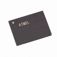
AT45DB642D-CNU Atmel, AT45DB642D-CNU Datasheet - Page 23

AT45DB642D-CNU
Manufacturer Part Number
AT45DB642D-CNU
Description
IC FLASH 64MBIT 66MHZ 8CASON
Manufacturer
Atmel
Datasheet
1.AT45DB642D-CU.pdf
(58 pages)
Specifications of AT45DB642D-CNU
Format - Memory
FLASH
Memory Type
DataFLASH
Memory Size
64M (8192 pages x 1056 bytes)
Speed
66MHz
Interface
Parallel/Serial
Voltage - Supply
2.7 V ~ 3.6 V
Operating Temperature
-40°C ~ 85°C
Package / Case
8-CASON
Package
8CASON
Density
64 Mb
Architecture
Sectored
Block Organization
Symmetrical
Typical Operating Supply Voltage
3.3 V
Sector Size
256KByte x 32
Timing Type
Synchronous
Interface Type
Parallel|Serial-SPI
Data Bus Width
8 bit
Supply Voltage (max)
3.6 V
Supply Voltage (min)
2.7 V
Maximum Operating Current
15 mA
Mounting Style
SMD/SMT
Organization
256 KB x 32
Ic Interface Type
Parallel, Serial
Clock Frequency
66MHz
Supply Voltage Range
2.7V To 3.6V
No. Of Pins
8
Operating Temperature Range
-40°C To +85°C
Rohs Compliant
Yes
Lead Free Status / RoHS Status
Lead free / RoHS Compliant
Available stocks
Company
Part Number
Manufacturer
Quantity
Price
Company:
Part Number:
AT45DB642D-CNU
Manufacturer:
MICRON
Quantity:
1 001
Company:
Part Number:
AT45DB642D-CNU
Manufacturer:
Atmel
Quantity:
59
Company:
Part Number:
AT45DB642D-CNU
Manufacturer:
AMTEL
Quantity:
143
Part Number:
AT45DB642D-CNU
Manufacturer:
ATMEL/爱特梅尔
Quantity:
20 000
Company:
Part Number:
AT45DB642D-CNU SL954
Manufacturer:
ATMEL
Quantity:
200
Part Number:
AT45DB642D-CNU SL954
Manufacturer:
ATMEL/爱特梅尔
Quantity:
20 000
Company:
Part Number:
AT45DB642D-CNU-SL954
Manufacturer:
PAM
Quantity:
34 000
11.4
3542K–DFLASH–04/09
Status Register Read
If a sector is programmed or reprogrammed sequentially page by page, then the programming
algorithm shown in
page or several pages are programmed randomly in a sector, then the programming algorithm
shown in
updated/rewritten at least once within every 10,000 cumulative page erase/program operations
in that sector.
The status register can be used to determine the device’s ready/busy status, page size, a Main
Memory Page to Buffer Compare operation result, the Sector Protection status or the device
density. To read the status register, an opcode of D7H must be loaded into the device. After the
opcode is clocked in, the 1-byte status register will be clocked out on the output pins (SO or
I/O7 - I/O0), starting with the next clock cycle. In case of applications with 8-bit interface, opcode
D7H and two dummy clock cycles should be used. When using the serial interface, the data in
the status register, starting with the MSB (bit 7), will be clocked out on the SO pin during the next
eight clock cycles. After the one byte of the status register has been clocked out, the sequence
will repeat itself (as long as CS remains low and SCK/CLK is being toggled). The data in the sta-
tus register is constantly updated, so each repeating sequence will output new data.
Ready/busy status is indicated using bit 7 of the status register. If bit 7 is a 1, then the device is
not busy and is ready to accept the next command. If bit 7 is a 0, then the device is in a busy
state. Since the data in the status register is constantly updated, the user must toggle SCK/CLK
pin to check the ready/busy status. There are several operations that can cause the device to be
in a busy state: Main Memory Page to Buffer Transfer, Main Memory Page to Buffer Compare,
Buffer to Main Memory Page Program, Main Memory Page Program through Buffer, Page
Erase, Block Erase, Sector Erase, Chip Erase and Auto Page Rewrite.
The result of the most recent Main Memory Page to Buffer Compare operation is indicated using
bit 6 of the status register. If bit 6 is a 0, then the data in the main memory page matches the
data in the buffer. If bit 6 is a 1, then at least one bit of the data in the main memory page does
not match the data in the buffer.
Bit 1 in the Status Register is used to provide information to the user whether or not the sector
protection has been enabled or disabled, either by software-controlled method or hardware-con-
trolled method. A logic 1 indicates that sector protection has been enabled and logic 0 indicates
that sector protection has been disabled.
Bit 0 in the Status Register indicates whether the page size of the main memory array is config-
ured for “power of 2” binary page size (1024 bytes) or standard DataFlash page size
(1056 bytes). If bit 0 is a 1, then the page size is set to 1024 bytes. If bit 0 is a 0, then the page
size is set to 1056 bytes.
The device density is indicated using bits 5, 4, 3, and 2 of the status register. For the
AT45DB642D, the four bits are 1111 The decimal value of these four binary bits does not equate
to the device density; the four bits represent a combinational code relating to differing densities
of DataFlash devices. The device density is not the same as the density code indicated in the
JEDEC device ID information. The device density is provided only for backward compatibility.
Table 11-1.
RDY/BUSY
Bit 7
Figure 26-2 (page
Status Register Format
COMP
Bit 6
Figure 26-1 (page
Bit 5
1
50) is recommended. Each page within a sector must be
Bit 4
1
49) is recommended. Otherwise, if multiple bytes in a
Bit 3
1
Bit 2
1
PROTECT
Bit 1
PAGE SIZE
Bit 0
23


