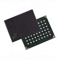
MT45W4MW16BFB-708 WT TR Micron Technology Inc, MT45W4MW16BFB-708 WT TR Datasheet - Page 9

MT45W4MW16BFB-708 WT TR
Manufacturer Part Number
MT45W4MW16BFB-708 WT TR
Description
IC PSRAM 64MBIT 70NS 54VFBGA
Manufacturer
Micron Technology Inc
Datasheet
1.MT45W4MW16BBB-706_WT_TR.pdf
(61 pages)
Specifications of MT45W4MW16BFB-708 WT TR
Format - Memory
RAM
Memory Type
PSRAM (Page)
Memory Size
64M (4M x 16)
Speed
70ns
Interface
Parallel
Voltage - Supply
1.7 V ~ 1.95 V
Operating Temperature
-30°C ~ 85°C
Package / Case
54-VFBGA
Lead Free Status / RoHS Status
Contains lead / RoHS non-compliant
Functional Description
Power-Up Initialization
Figure 4:
Bus Operating Modes
Asynchronous Mode
PDF: 09005aef80be1fbd/Source: 09005aef80be2036
Burst CellularRAM_2.fm - Rev. G 10/05 EN
Power-Up Initialization Timing
In general, the MT45W4MW16BFB device is a high-density alternative to SRAM and
Pseudo SRAM products, popular in low-power, portable applications.
The MT45W4MW16BFB device contains a 67,108,864-bit DRAM core, organized as
4,194,304 addresses by 16 bits. The device implements the same high-speed bus inter-
face found on burst mode Flash products.
The CellularRAM bus interface supports both asynchronous and burst mode transfers.
Page mode accesses are also included as a bandwidth-enhancing extension to the asyn-
chronous read protocol.
CellularRAM products include an on-chip voltage sensor used to launch the power-up
initialization process. Initialization will configure the BCR and the RCR with their default
settings (see Table 17 on page 21 and Table 22 on page 26). V
applied simultaneously. When they reach a stable level at or above 1.70V, the device will
require 150µs to complete its self-initialization process. During the initialization period,
CE# should remain HIGH. When initialization is complete, the device is ready for nor-
mal operation.
VccQ
The MT45W4MW16BFB CellularRAM product incorporates a burst mode interface
found on Flash products targeting low-power, wireless applications. This bus interface
supports asynchronous, page mode, and burst mode read and write transfers. The spe-
cific interface supported is defined by the value loaded into the BCR. Page mode is con-
trolled by the refresh configuration register (RCR[7]).
CellularRAM products power up in the asynchronous operating mode. This mode uses
the industry-standard SRAM control bus (CE#, OE#, WE#, LB#/UB#). READ operations
(Figure 5) are initiated by bringing CE#, OE#, and LB#/UB# LOW while keeping WE#
HIGH. Valid data will be driven out of the I/Os after the specified access time has
elapsed. WRITE operations (Figure 6) occur when CE#, WE#, and LB#/UB# are driven
LOW. During asynchronous WRITE operations, the OE# level is a “Don’t Care,” and WE#
will override OE#. The data to be written is latched on the rising edge of CE#, WE#, or
LB#/UB# (whichever occurs first). Asynchronous operations (page mode disabled) can
either use the ADV input to latch the address, or ADV can be driven LOW during the
entire READ/WRITE operation.
During asynchronous operation, the CLK input must be static (HIGH or LOW—no tran-
sitions). WAIT will be driven while the device is enabled and its state should be ignored.
WE# LOW time must be limited to
Vcc
Vcc = 1.70V
64Mb: 4 Meg x 16 Async/Page/Burst CellularRAM 1.0 Memory
Device Initialization
t PU > 150µs
9
t
CEM.
Device ready for
normal operation
Micron Technology, Inc., reserves the right to change products or specifications without notice.
Functional Description
CC
©2003 Micron Technology, Inc. All rights reserved.
and V
CC
Q must be


