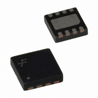
FAN3224TMPX Fairchild Semiconductor, FAN3224TMPX Datasheet - Page 18

FAN3224TMPX
Manufacturer Part Number
FAN3224TMPX
Description
IC GATE DVR DUAL 4A 8-MLP
Manufacturer
Fairchild Semiconductor
Type
Low Sider
Datasheet
1.FAN3223TMX.pdf
(25 pages)
Specifications of FAN3224TMPX
Configuration
Low-Side
Input Type
Non-Inverting
Delay Time
17ns
Current - Peak
5A
Number Of Configurations
2
Number Of Outputs
2
Voltage - Supply
4.5 V ~ 18 V
Operating Temperature
-40°C ~ 125°C
Mounting Type
Surface Mount
Package / Case
8-MLP
Rise Time
20 ns
Fall Time
17 ns
Supply Voltage (min)
4.5 V
Supply Current
0.95 mA
Maximum Operating Temperature
+ 125 C
Mounting Style
SMD/SMT
Minimum Operating Temperature
- 40 C
Number Of Drivers
2
Lead Free Status / RoHS Status
Lead free / RoHS Compliant
High Side Voltage - Max (bootstrap)
-
Lead Free Status / Rohs Status
Lead free / RoHS Compliant
Other names
FAN3224TMPXTR
Available stocks
Company
Part Number
Manufacturer
Quantity
Price
Part Number:
FAN3224TMPX
Manufacturer:
FAIRCHILD/仙童
Quantity:
20 000
© 2007 Fairchild Semiconductor Corporation
FAN3223 / FAN3224 / FAN3225 • Rev. 1.0.6
VDD Bypass Capacitor Guidelines
To enable this IC to turn a device ON quickly, a local
high-frequency bypass capacitor C
ESL should be connected between the VDD and GND
pins with minimal trace length. This capacitor is in
addition to bulk electrolytic capacitance of 10µF to 47µF
commonly found on driver and controller bias circuits.
A typical criterion for choosing the value of C
keep the ripple voltage on the V
is often achieved with a value ≥20 times the equivalent
load capacitance C
Ceramic capacitors of 0.1µF to 1µF or larger are
common choices, as are dielectrics, such as X5R and
X7R with good temperature characteristics and high
pulse current capability.
If circuit noise affects normal operation, the value of
C
C
larger value, based on equivalent load capacitance, and
the other a smaller value, such as 1-10nF mounted
closest to the VDD and GND pins to carry the higher
frequency components of the current pulses. The
bypass capacitor must provide the pulsed current from
both of the driver channels and, if the drivers are
switching simultaneously, the combined peak current
sourced from the C
a single channel is switching.
Layout and Connection Guidelines
The FAN3223-25 family of gate drivers incorporates
fast-reacting input circuits, short propagation delays,
and powerful output stages capable of delivering current
peaks over 4A to facilitate voltage transition times from
under 10ns to over 150ns. The following layout and
connection guidelines are strongly recommended:
BYP
BYP
Keep high-current output and power ground paths
separate logic and enable input signals and signal
ground paths. This is especially critical when
dealing with TTL-level logic thresholds at driver
inputs and enable pins.
Keep the driver as close to the load as possible to
minimize the length of high-current traces. This
reduces the series inductance to improve high-
speed switching, while reducing the loop area that
can radiate EMI to the driver inputs and
surrounding circuitry.
If the inputs to a channel are not externally
connected, the internal 100k resistors indicated
on block diagrams command a low output. In noisy
environments, it may be necessary to tie inputs of
an unused channel to VDD or GND using short
traces to prevent noise from causing spurious
output switching.
Many high-speed power circuits can be susceptible
to noise injected from their own output or other
external sources, possibly causing output re-
triggering. These effects can be obvious if the
circuit is tested in breadboard or non-optimal circuit
layouts with long input, enable, or output leads. For
best results, make connections to all pins as short
and direct as possible.
may be split into two capacitors. One should be a
may be increased to 50-100 times the C
BYP
EQV
would be twice as large as when
, defined here as Q
DD
BYP
supply to ≤5%. This
with low ESR and
GATE
BYP
EQV
/V
is to
, or
DD
.
18
Figure 48 shows the pulsed gate drive current path
when the gate driver is supplying gate charge to turn the
MOSFET ON. The current is supplied from the local
bypass capacitor, C
the MOSFET gate and to ground. To reach the high
peak currents possible, the resistance and inductance in
the path should be minimized. The localized C
to contain the high peak current pulses within this driver-
MOSFET circuit, preventing them from disturbing the
sensitive analog circuitry in the PWM controller.
Figure 49 shows the current path when the gate driver
turns the MOSFET OFF. Ideally, the driver shunts the
current directly to the source of the MOSFET in a small
circuit loop. For fast turn-off times, the resistance and
inductance in this path should be minimized.
Figure 49. Current Path for MOSFET Turn-off
Figure 48. Current Path for MOSFET Turn-on
The FAN322x is compatible with many other
industry-standard drivers. In single input parts with
enable pins, there is an internal 100k resistor tied
to VDD to enable the driver by default; this should
be considered in the PCB layout.
The turn-on and turn-off current paths should be
minimized, as discussed in the following section.
PWM
C
BYP
BYP
, and flows through the driver to
V
DD
FAN322x
www.fairchildsemi.com
V
DS
BYP
acts


