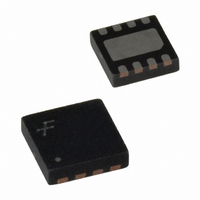
FAN3224TMPX Fairchild Semiconductor, FAN3224TMPX Datasheet - Page 6

FAN3224TMPX
Manufacturer Part Number
FAN3224TMPX
Description
IC GATE DVR DUAL 4A 8-MLP
Manufacturer
Fairchild Semiconductor
Type
Low Sider
Datasheet
1.FAN3223TMX.pdf
(25 pages)
Specifications of FAN3224TMPX
Configuration
Low-Side
Input Type
Non-Inverting
Delay Time
17ns
Current - Peak
5A
Number Of Configurations
2
Number Of Outputs
2
Voltage - Supply
4.5 V ~ 18 V
Operating Temperature
-40°C ~ 125°C
Mounting Type
Surface Mount
Package / Case
8-MLP
Rise Time
20 ns
Fall Time
17 ns
Supply Voltage (min)
4.5 V
Supply Current
0.95 mA
Maximum Operating Temperature
+ 125 C
Mounting Style
SMD/SMT
Minimum Operating Temperature
- 40 C
Number Of Drivers
2
Lead Free Status / RoHS Status
Lead free / RoHS Compliant
High Side Voltage - Max (bootstrap)
-
Lead Free Status / Rohs Status
Lead free / RoHS Compliant
Other names
FAN3224TMPXTR
Available stocks
Company
Part Number
Manufacturer
Quantity
Price
Part Number:
FAN3224TMPX
Manufacturer:
FAIRCHILD/仙童
Quantity:
20 000
© 2007 Fairchild Semiconductor Corporation
FAN3223 / FAN3224 / FAN3225 • Rev. 1.0.6
Absolute Maximum Ratings
Stresses exceeding the absolute maximum ratings may damage the device. The device may not function or be
operable above the recommended operating conditions and stressing the parts to these levels is not recommended.
In addition, extended exposure to stresses above the recommended operating conditions may affect device reliability.
The absolute maximum ratings are stress ratings only.
Recommended Operating Conditions
The Recommended Operating Conditions table defines the conditions for actual device operation. Recommended
operating conditions are specified to ensure optimal performance to the datasheet specifications. Fairchild does not
recommend exceeding them or designing to Absolute Maximum Ratings.
Symbol
Symbol
V
ESD
T
V
V
V
V
V
V
T
T
T
STG
OUT
DD
DD
EN
EN
IN
IN
A
L
J
VDD to PGND
ENA and ENB to GND
INA, INA+, INA–, INB, INB+ and INB– to GND
OUTA and OUTB to GND
Lead Soldering Temperature (10 Seconds)
Junction Temperature
Storage Temperature
Electrostatic Discharge
Protection Level
Supply Voltage Range
Enable Voltage ENA and ENB
Input Voltage INA, INA+, INA–, INB, INB+ and INB–
Operating Ambient Temperature
Human Body Model, JEDEC JESD22-A114
Charged Device Model, JEDEC JESD22-C101
Parameter
Parameter
6
GND - 0.3 V
GND - 0.3 V
GND - 0.3 V
Min.
Min.
-40
4.5
-0.3
-55
-65
0
0
4
1
Max.
+125
18.0
V
V
DD
DD
DD
Max.
+260
+150
+150
DD
DD
20.0
www.fairchildsemi.com
+ 0.3
+ 0.3
+ 0.3
Unit
Unit
ºC
V
V
V
ºC
ºC
kV
kV
ºC
V
V
V
V


