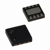
FAN3224TMPX Fairchild Semiconductor, FAN3224TMPX Datasheet - Page 19

FAN3224TMPX
Manufacturer Part Number
FAN3224TMPX
Description
IC GATE DVR DUAL 4A 8-MLP
Manufacturer
Fairchild Semiconductor
Type
Low Sider
Datasheet
1.FAN3223TMX.pdf
(25 pages)
Specifications of FAN3224TMPX
Configuration
Low-Side
Input Type
Non-Inverting
Delay Time
17ns
Current - Peak
5A
Number Of Configurations
2
Number Of Outputs
2
Voltage - Supply
4.5 V ~ 18 V
Operating Temperature
-40°C ~ 125°C
Mounting Type
Surface Mount
Package / Case
8-MLP
Rise Time
20 ns
Fall Time
17 ns
Supply Voltage (min)
4.5 V
Supply Current
0.95 mA
Maximum Operating Temperature
+ 125 C
Mounting Style
SMD/SMT
Minimum Operating Temperature
- 40 C
Number Of Drivers
2
Lead Free Status / RoHS Status
Lead free / RoHS Compliant
High Side Voltage - Max (bootstrap)
-
Lead Free Status / Rohs Status
Lead free / RoHS Compliant
Other names
FAN3224TMPXTR
Available stocks
Company
Part Number
Manufacturer
Quantity
Price
Part Number:
FAN3224TMPX
Manufacturer:
FAIRCHILD/仙童
Quantity:
20 000
© 2007 Fairchild Semiconductor Corporation
FAN3223 / FAN3224 / FAN3225 • Rev. 1.0.6
Truth Table of Logic Operation
The FAN3225 truth table indicates the operational states
using the dual-input configuration. In a non-inverting
driver configuration, the IN- pin should be a logic LOW
signal. If the IN- pin is connected to logic HIGH, a disable
function is realized, and the driver output remains LOW
regardless of the state of the IN+ pin.
In the non-inverting driver configuration in Figure 50, the
IN- pin is tied to ground and the input signal (PWM) is
applied to IN+ pin. The IN- pin can be connected to logic
HIGH to disable the driver and the output remains LOW,
regardless of the state of the IN+ pin.
In the inverting driver application in Figure 51, the IN+
pin is tied HIGH. Pulling the IN+ pin to GND forces the
output LOW, regardless of the state of the IN- pin.
IN+
Figure 50. Dual-Input Driver Enabled,
Figure 51. Dual-Input Driver Enabled,
0
0
1
1
Non-Inverting Configuration
Inverting Configuration
IN-
0
1
0
1
OUT
0
0
1
0
19
Operational Waveforms
At power-up, the driver output remains LOW until the
V
magnitude of the OUT pulses rises with V
steady-state
operation illustrated in Figure 52 shows that the output
remains LOW until the UVLO threshold is reached, then
the output is in-phase with the input.
For the inverting configuration of Figure 51, start-up
waveforms are shown in Figure 53. With IN+ tied to
VDD and the input signal applied to IN–, the OUT
pulses are inverted with respect to the input. At power-
up, the inverted output remains LOW until the V
voltage reaches the turn-on threshold, then it follows the
input with inverted phase.
DD
Figure 52. Non-Inverting Start-Up Waveforms
voltage reaches the turn-on threshold. The
Figure 53. Inverting Start-Up Waveforms
V
DD
is
reached.
The
www.fairchildsemi.com
non-inverting
DD
until
DD


