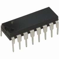
FAN4800IN Fairchild Semiconductor, FAN4800IN Datasheet - Page 11

FAN4800IN
Manufacturer Part Number
FAN4800IN
Description
IC PFC CONTROLLER CCM/DCM 16DIP
Manufacturer
Fairchild Semiconductor
Specifications of FAN4800IN
Mode
Continuous Conduction (CCM), Discontinuous Conduction (DCM)
Frequency - Switching
66kHz ~ 84kHz
Current - Startup
100µA
Voltage - Supply
11 V ~ 16.5 V
Operating Temperature
-40°C ~ 125°C
Mounting Type
Through Hole
Package / Case
16-DIP (0.300", 7.62mm)
Mounting Style
Through Hole
Lead Free Status / RoHS Status
Lead free / RoHS Compliant
Available stocks
Company
Part Number
Manufacturer
Quantity
Price
Part Number:
FAN4800IN
Manufacturer:
FSC
Quantity:
20 000
FAN4800 Rev. 1.0.5
© 2005 Fairchild Semiconductor Corporation
1.6 Error Amplifier Compensation
The PWM loading of the PFC can be modeled as a neg-
ative resistor because an increase in the input voltage to
the PWM causes a decrease in the input current. This
response dictates the proper compensation of the two
transconductance error amplifiers.
Figure 8 shows the types of compensation networks
most commonly used for the voltage and current error
amplifiers, along with their respective return points. The
current-loop compensation is returned to V
duce a soft-start characteristic on the PFC: As the refer-
ence
differentiated voltage on I
from immediately demanding a full duty cycle on its
boost converter.
1.7 PFC Voltage Loop
There are two major concerns when compensating the
voltage loop error amplifier (V
response. Optimizing interaction between transient
response and stability requires that the error amplifier’s
open-loop crossover frequency half that of the line fre-
quency, or 23Hz for a 47Hz line (lowest anticipated inter-
national power frequency). The gain vs. input voltage of
the FAN4800’s voltage error amplifier (V
cially shaped non-linearity, so that under steady-state
operating conditions, the transconductance of the error
amplifier is at a local minimum. Rapid perturbation in line
or load conditions causes the input to the voltage error
amplifier (V
this happens, the transconductance of the voltage error
amplifier increases significantly, as shown in the Figure
4. This raises the gain-bandwidth product of the voltage
loop, resulting in a much more rapid voltage loop
response to such perturbations than would occur with
conventional linear gain characteristics.
15
2
4
3
7
V
V
I
2.5V
RAMP1
I
AC
voltage
SENSE
FB
RMS
FB
) to deviate from its 2.5V (nominal) value. If
V
EAO
increases
MODULATOR
GAIN
16
0.3V
EAO
from
EAO
, which prevents the PFC
3.5k
3.5k
); stability and transient
Low Power
Detector
0V,
I
EAO
Figure 7. PFC Section Block Diagram
EAO
it
1
) has a spe-
REF
creates
17.9V
PFC CMP
OSCILLATOR
V
0.5V
to pro-
CC
POWER FACTOR CORRECTOR
TRI-FAULT
a
11
V
CC
The Voltage loop gain(s) is given by:
where:
Z
GM
P
V
C
1.8 PFC Current Loop
The compensation of the current amplifier (I
lar to that of the voltage error amplifier (V
exception of the choice of crossover frequency. The
crossover frequency of the current amplifier should be at
least ten times that of the voltage amplifier to prevent
interaction with the voltage loop. It should also be limited
to less than one sixth of the switching frequency, e.g.,
16.7kHz for a 100kHz switching frequency.
The current loop gain(s) is given by:
C
IN
2
OVP
DC
OUTDC
:
:
V
:
2.78V
:
-1V
≈
: PFC boost output voltage (typical designed
value is 380V).
Transconductance of V
V
PFC boost output capacitor.
Compensation network for the voltage loop.
Average PFC input power.
2
OUTDC
=
=
Δ
PFC OVP
≈
Δ
V
Δ
Δ
ISENSE
D
V
S L
V
V
P
OUTDC
OFF
PFC I
× Δ
OUT
EAO
IN
× ×
×
V
EAO
2.5
×
×
2.5
LIMIT
×
Δ
Δ
Δ
Δ
V
R
V
× ×
D
V
I
V
S
OUT
EAO
OFF
S C
FB
×
GM
×
×
DC
Δ
Δ
REFERENCE
I
Δ
EAO
V
V
×
S
R
S
R
Δ
V
×
EAO
ISENSE
I
Z
FB
7.5V
GM
EAO
CI
13
.
Q
Q
V
V
CC
×
FAN4800 Rev.02
Z
EAO
www.fairchildsemi.com
CLK
C
PFC OUT
EAO
V
) with the
REF
) is simi-
14
12
(6)
(7)


