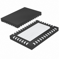
LTC3735EUHF Linear Technology, LTC3735EUHF Datasheet - Page 10

LTC3735EUHF
Manufacturer Part Number
LTC3735EUHF
Description
IC CTRLR DC/DC 2PH HI EFF 38-QFN
Manufacturer
Linear Technology
Datasheet
1.LTC3735EG.pdf
(32 pages)
Specifications of LTC3735EUHF
Applications
Controller, Intel Mobile CPU
Number Of Outputs
1
Voltage - Output
0.7 ~ 1.71 V
Operating Temperature
-40°C ~ 85°C
Mounting Type
Surface Mount
Package / Case
38-QFN
Lead Free Status / RoHS Status
Contains lead / RoHS non-compliant
Voltage - Input
-
Available stocks
Company
Part Number
Manufacturer
Quantity
Price
Company:
Part Number:
LTC3735EUHF
Manufacturer:
LT
Quantity:
10 000
Part Number:
LTC3735EUHF#PBF
Manufacturer:
LINEAR/凌特
Quantity:
20 000
LTC3735
OPERATIO
Main Control Loop
The LTC3735 uses a constant frequency, current mode
step-down architecture with the two output stages oper-
ating 180 degrees out of phase. During normal operation,
each top MOSFET is turned on when the clock for that
channel sets the RS latch, and turned off when the main
current comparator, I
inductor current at which I
trolled by the voltage on the I
error amplifier EA. The V
feedback signal, which is compared to the internal refer-
ence voltage by the EA. When the load current increases,
it causes a slight decrease in EA inverting input node
relative to the 0.6V reference, which in turn causes the I
voltage to increase until the average inductor current
matches the new load current. After the top MOSFET has
turned off, the bottom MOSFET is turned on until either the
inductor current starts to reverse, as indicated by current
comparator I
The top MOSFET drivers are biased from floating boot-
strap capacitor C
each off cycle through an external diode when the top
MOSFET turns off. As V
V
the top MOSFET continuously. The dropout detector de-
tects this and forces the top MOSFET off for about 500ns
every sixth cycle to allow C
The main control loop is shut down by pulling the RUN/
SS pin low. Releasing RUN/SS allows an internal 1.5μA
current source to charge soft-start capacitor C
C
the internal I
its maximum value. As C
internal I
full-current operation.
Frequency Programming and Antiphase Operation
The switching frequency of the LTC3735 is determined by
the DC voltage at the FREQSET pin. A DC voltage ranging
from 0V to 2.4V moves the internal oscillator frequency
from 210kHz to 550kHz.
10
OUT
SS
reaches 1.5V, the main control loop is enabled with
, the loop may enter dropout and attempt to turn on
TH
voltage is gradually released allowing normal,
TH
2
, or the beginning of the next cycle.
voltage clamped at approximately 30% of
B
U
, which normally is recharged during
1
(Refer to Functional Diagram)
, resets the RS latch. The peak
IN
decreases to a voltage close to
OA
B
SS
1
TH
to recharge.
resets the RS latch is con-
+
continues to charge, the
pin, which is the output of
pin receives the voltage
SS
. When
TH
This frequency is the actual switching frequency of either
channel. Because the two channels operate 180°C out of
phase, the apparent frequency at both V
twice the actual switching frequency, minimizing ripple
voltages and speeding up transient responses.
Low Current Operation (PSIB)
The PSIB pin selects between two modes of operation.
When PSIB is above 0.6V, both channels operate in full
synchronous switching mode. Both bottom drivers (BG1,
BG2) are kept on once they are turned on until their
respective oscillator sets the RS latch. The inductor cur-
rent can therefore go from output back to input power
supply and could potentially boost the input supply to
dangerous voltage levels—BEWARE! This mode of opera-
tion is also of lower efficiency, given both channels are
fully enabled and much current can circulate between
input and output. However, this mode provides faster
transient response, lower input noise and minimum out-
put ripple.
When PSIB is below 0.6V, the bottom drivers (BG1, BG2)
are turned off if the inductor current starts to reverse. This
mode of operation prevents current going from output
back to input and eliminates the conduction power loss
related to circulating current. If the DPRSLPVR signal
goes high in this mode, Channel 2 will be shut off and only
Channel 1 will be active in supplying load current. This
further eliminates power MOSFET gate driving and tran-
sition losses of Channel 2. Since DPRSLPVR indicates the
entry to deeper sleep state, this “channel shedding”
technique optimizes the voltage regulator efficiency at
light loads. Table 1 summarizes the operation modes for
different pin configurations.
Table 1. Low Current Operation Modes
PSIB
High
Low
Low
High or Low
DPRSLPVR
High
Low
OPERATION MODE
Switching,Inductor Current is Allowed to
Reverse
Both Channels ON; Reverse Current is
Prevented
Prevented
Both Channels ON, Fully Synchronous
Channel 2 is Shut Off, Reverse Current is
IN
and V
OUT
3735f
is


