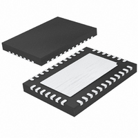
LTC3735EUHF Linear Technology, LTC3735EUHF Datasheet - Page 7

LTC3735EUHF
Manufacturer Part Number
LTC3735EUHF
Description
IC CTRLR DC/DC 2PH HI EFF 38-QFN
Manufacturer
Linear Technology
Datasheet
1.LTC3735EG.pdf
(32 pages)
Specifications of LTC3735EUHF
Applications
Controller, Intel Mobile CPU
Number Of Outputs
1
Voltage - Output
0.7 ~ 1.71 V
Operating Temperature
-40°C ~ 85°C
Mounting Type
Surface Mount
Package / Case
38-QFN
Lead Free Status / RoHS Status
Contains lead / RoHS non-compliant
Voltage - Input
-
Available stocks
Company
Part Number
Manufacturer
Quantity
Price
Company:
Part Number:
LTC3735EUHF
Manufacturer:
LT
Quantity:
10 000
Part Number:
LTC3735EUHF#PBF
Manufacturer:
LINEAR/凌特
Quantity:
20 000
PI FU CTIO S
V
compares the feedback voltage to the internal 0.6V refer-
ence voltage.
DPRSLPVR (Pin 2/Pin 38): Deeper Sleep State Input.
When the signal to this pin is high, the voltage regulator
enters deeper sleep state and its output is determined by
the parallel resistor value of RDPRSLP and RDPSLP.
When the signal is low, the voltage regulator exits deeper
sleep state.
FREQSET (Pin 3/Pin 1): Frequency Set Pin. Apply a DC
voltage between 0V and 5V to set the operating frequency
of the internal oscillator. This frequency is the switching
frequency of each phase.
PSIB (Pin 4/Pin 2): Power Status Indicator Input. When
the signal to this pin is high, both channels operate in fully
synchronous switching mode for fastest transient and
lowest ripple. When the signal is low, controller enters
power saving mode, providing high efficiency at light load.
V
Operational Amplifier.
OAOUT (Pin 7/Pin 5): Output of the Internal Operational
Amplifier.
TYPICAL PERFOR A CE CHARACTERISTICS
FB
OA
3.0
2.5
2.0
1.0
4.5
4.0
3.5
1.5
0.5
U
0
+
–50
(Pin 1/Pin 37): Input to the error amplifier that
, V
V
Thresholds vs Temperature
RUN/SS
OA
–25
–
U
(Pins 5, 6/Pins 3, 4): Inputs to the Internal
Shutdown Latch
0
TEMPERATURE (°C)
THRESHOLD
LATCHOFF
25
LATCH ARMING
U
50
75
W
G Package/UHF Package
100
3735 G21
U
125
100mV/DIV
10A/DIV
1.364V
1.230V
V
I
7.2A
OUT
32A
OUT
Load Step (Figure 14)
20μs/DIV
STP_CPUB (Pin 8/Pin 6): Deep Sleep State Input. When
the signal to this pin is low, the voltage regulator enters
deep sleep state and its output voltage is a certain percent-
age lower than the VID commands. This offset percentage
is set by the resistor connected to the RDPSLP pin. When
the signal to this pin is high, the voltage regulator exits
deep sleep state.
SGND (Pin 9/Pin 7): Signal Ground. This pin is common
to both controllers. Route separately to the PGND pin.
SENSE1
to Each Differential Current Comparator. The I
voltage and built-in offsets between SENSE
pins in conjunction with R
threshold.
SENSE1
Input to Each Differential Current Comparator.
RDPRSLP (Pin 14/Pin 12): Deeper Sleep State Resistor
Pin. Connect a resistor from this pin to V
in conjunction with RDPSLP resistor sets the output
voltage of the regulator in deeper sleep state.
RDPSLP (Pin 15/Pin 14): Deep Sleep Resistor Pin. Con-
nect a resistor from this pin to V
percentage offset of output voltage in deep sleep state.
–
+
, SENSE2
, SENSE2
3735 G22
+
–
200mV
PGOOD
(Pins 10,12/Pins 8, 9): The (+) Input
VIDs
1.356V
0.844V
2V/DIV
(Pins 11,13/Pins 10, 11): The (–)
V
/DIV
OUT
1
0
VID Transition (Figure 14)
SENSE
OA
+
. This resistor sets the
set the current trip
50μs/DIV
OA
LTC3735
+
–
. This resistor
and SENSE
TH
3735 G23
7
3735f
pin
+


