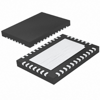
LTC3735EUHF Linear Technology, LTC3735EUHF Datasheet - Page 17

LTC3735EUHF
Manufacturer Part Number
LTC3735EUHF
Description
IC CTRLR DC/DC 2PH HI EFF 38-QFN
Manufacturer
Linear Technology
Datasheet
1.LTC3735EG.pdf
(32 pages)
Specifications of LTC3735EUHF
Applications
Controller, Intel Mobile CPU
Number Of Outputs
1
Voltage - Output
0.7 ~ 1.71 V
Operating Temperature
-40°C ~ 85°C
Mounting Type
Surface Mount
Package / Case
38-QFN
Lead Free Status / RoHS Status
Contains lead / RoHS non-compliant
Voltage - Input
-
Available stocks
Company
Part Number
Manufacturer
Quantity
Price
Company:
Part Number:
LTC3735EUHF
Manufacturer:
LT
Quantity:
10 000
Part Number:
LTC3735EUHF#PBF
Manufacturer:
LINEAR/凌特
Quantity:
20 000
APPLICATIO S I FOR ATIO
In surface mount applications, multiple capacitors may
have to be paralleled to meet the ESR or RMS current
handling requirements of the application. Aluminum elec-
trolytic and dry tantalum capacitors are both available in
surface mount configurations. New special polymer (SP)
surface mount capacitors from Panasonic offer very low
ESR also but have much lower capacitive density per unit
volume. In the case of tantalum, it is critical that the
capacitors are surge tested for use in switching power
supplies. Several excellent choices are the AVX TPS, AVX
TPSV or the KEMET T510 series of surface mount
tantalums, available in case heights ranging from 2mm to
4mm. Other capacitor types include Sanyo OS-CON,
POSCAPs, Kemet AO-CAPs , Nichicon PL series and
Sprague 595D series. Consult the manufacturer for other
specific recommendations. A combination of capacitors
will often result in maximizing performance and minimiz-
ing overall cost and size.
PV
The PV
drivers and therefore must be bypassed to power ground
with a minimum of 4.7μF ceramic or tantalum capacitor.
Since the gate driving currents are of high amplitude and
high slew rate, this bypassing capacitor should be placed
very close to the PV
parasitic inductance. Do NOT apply greater than 7V to the
PV
The PV
circuitry of the LTC3735. This supply current is much
lower than that of the current for the external MOSFET
gate drive. Ceramic capacitors are very good for high
frequency filtering and a 0.1μF ~ 1μF ceramic capacitor
should be placed adjacent to the PV
Topside MOSFET Driver Supply (C
Functional Diagram)
External bootstrap capacitors C
the BOOST1 and BOOST2 pins supply the gate drive
voltages for the topside MOSFETs. Capacitor C
CC
CC
Decoupling
pin.
CC
CC
pin also supplies current to the internal control
pin supplies power to the top and bottom gate
U
CC
and PGND pins to minimize the
U
B1
and C
W
B
CC
,D
B
and SGND pins.
) (Refer to
B2
connected to
U
B
in the
Functional Diagram is charged though diode D
when the SW pin is low. When the topside MOSFET turns
on, the driver places the C
of the desired MOSFET. This enhances the MOSFET and
turns on the topside switch. The switch node voltage, SW,
rises to V
value of the boost capacitor C
that of the total input capacitance of the topside MOSFET(s).
The reverse breakdown of D
PV
VID Output Voltage Programming
After 27μs ~ 71μs t
regulator is digitally programmed as defined in Table 2
using the VID0 to VID5 logic input pins. The VID logic
inputs program a precision, 0.25% internal feedback
resistive divider. The LTC3735 has an output voltage
range of 0.700V to 1.708V in 16mV steps.
Refering to the Functional Diagram, there is a resistor,
R
by the six VID input pins. Another internal resistor, 5.33k
(R
voltage is thus set by the ratio of (R
Each VID digital pin is a high impedance input. Therefore
they must be actively pulled high or pulled low. The logic
low threshold of the VID pins is 0.3V; the logic high
threshold is 0.7V.
Soft-Start/Run Function
The RUN/SS pin provides three functions: 1) run/shut-
down, 2) soft-start and 3) an optional short-circuit latchoff
timer. Soft-start reduces the input power sources’ surge
currents by gradually increasing the controller’s current
limit. The latchoff timer prevents very short, extreme load
transients from tripping the overcurrent latch. A small pull-
up current (>5μA) supplied to the RUN/SS pin will prevent
the overcurrent latch from operating. The following para-
graph describes how the functions operate.
VID
ATTEN
CC(MAX).
, from V
), completes the resistive divider. The output
IN
and the BOOST pin rises to V
FB
to ground. The value of R
BOOT
B
delay, the output voltage of the
voltage across the gate-source
B
needs to be 30 to 100 times
B
must be greater than
VID
+ 5.33k) to R
VID
LTC3735
IN
is controlled
+ PV
B
from PV
17
CC
. The
VID
3735f
CC
.


