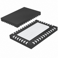
LTC3735EUHF Linear Technology, LTC3735EUHF Datasheet - Page 20

LTC3735EUHF
Manufacturer Part Number
LTC3735EUHF
Description
IC CTRLR DC/DC 2PH HI EFF 38-QFN
Manufacturer
Linear Technology
Datasheet
1.LTC3735EG.pdf
(32 pages)
Specifications of LTC3735EUHF
Applications
Controller, Intel Mobile CPU
Number Of Outputs
1
Voltage - Output
0.7 ~ 1.71 V
Operating Temperature
-40°C ~ 85°C
Mounting Type
Surface Mount
Package / Case
38-QFN
Lead Free Status / RoHS Status
Contains lead / RoHS non-compliant
Voltage - Input
-
Available stocks
Company
Part Number
Manufacturer
Quantity
Price
Company:
Part Number:
LTC3735EUHF
Manufacturer:
LT
Quantity:
10 000
Part Number:
LTC3735EUHF#PBF
Manufacturer:
LINEAR/凌特
Quantity:
20 000
APPLICATIO S I FOR ATIO
LTC3735
Output Voltage Set in Deep Sleep and Deeper Sleep
States (Refer to the Functional Diagram)
The output voltage can be offset by the STP_CPUB signal.
When STP_CPUB becomes low, the output voltage will be
a certain percentage lower than that set by the VID bits in
Table 2. This state is defined to be the deep sleep state.
Referring to the Functional Diagram, we can caluculate the
STP_CPUB offset to be:
By using different R4 resistors, STP_CPUB offset can be
programmed.
The output voltage could also be set by external resistors
R6 and R4 when DPRSLPVR input is high. This state is
defined to be the deeper sleep state. The output voltage
is set to V
By using different value R6 resistors, V
programmed.
(The digital input threshold voltage is set to 1.8V for
STP_CPUB, DPRSLPVR and MCH_PG inputs.)
Power Good Masking
The PGOOD output monitors V
within ±10% of the set point, PGOOD is pulled low with an
internal MOSFET. When V
window, PGOOD is high impedance. PGOOD should be
pulled up by an external resistor.
During VID changes, deep sleep and deeper sleep transi-
tions, the output voltage can initially be out of the ±10%
window of the newly set regulation point. To avoid nui-
sance indications from PGOOD, a timer masks PGOOD for
110μs. If V
20
STP
V
DPRSLPVR
% –
=
DPRSLPVR
OUT
R
=
is still out of regulation after this blanking
3
R
0 6
+
3
.
U
R
, regardless of the VID setting:
V
4
•
•
(
100
R
R
U
2
6
•
OUT
||
%
(
R
R
4
3
)
is within the regulation
OUT
+
•
(
R
W
R
. When V
6
1
||
+
R
DPRSLPVR
R
4
2
)
)
OUT
U
can be
is not
time, PGOOD goes low. Any overvoltage or undervoltage
condition is also masked for 110μs before it is reported by
PGOOD.
The masking circuitry also adaptively tracks VID and state
changes. If a new change in VID or state happens before
the 110μs masking timer expires, the timer resets and
starts a fresh count of 110μs. This prevents the system
from rebooting under frequent output voltage transitions.
Refer to Figure 8 for the PGOOD timing diagram.
During start-up, PGOOD is actively pulled low until the
RUN/SS pin voltage reaches its arming voltage, which is
4.2V typically, only then is the PGOOD pull-low signal
released. When RUN/SS goes low, PGOOD goes low
simultaneously.
Fault Conditions: Overcurrent Latchoff
The RUN/SS pin also provides the ability to latch off the
controller when an overcurrent condition is detected. The
RUN/SS capacitor, C
COMPARATOR)
POWER GOOD
INTERNAL PG
(OUTPUT OF
INTERNAL
MASKING
VID BITS
PGOOD
PGOOD
V
OUT
Figure 8. PGOOD Timing Diagram
SS
, is used initially to limit the inrush
110μs
TIME
110μs
3735 F08
3735f


