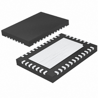
LTC3735EUHF Linear Technology, LTC3735EUHF Datasheet - Page 8

LTC3735EUHF
Manufacturer Part Number
LTC3735EUHF
Description
IC CTRLR DC/DC 2PH HI EFF 38-QFN
Manufacturer
Linear Technology
Datasheet
1.LTC3735EG.pdf
(32 pages)
Specifications of LTC3735EUHF
Applications
Controller, Intel Mobile CPU
Number Of Outputs
1
Voltage - Output
0.7 ~ 1.71 V
Operating Temperature
-40°C ~ 85°C
Mounting Type
Surface Mount
Package / Case
38-QFN
Lead Free Status / RoHS Status
Contains lead / RoHS non-compliant
Voltage - Input
-
Available stocks
Company
Part Number
Manufacturer
Quantity
Price
Company:
Part Number:
LTC3735EUHF
Manufacturer:
LT
Quantity:
10 000
Part Number:
LTC3735EUHF#PBF
Manufacturer:
LINEAR/凌特
Quantity:
20 000
PI FU CTIO S
RUN/SS (Pin 16/Pin 15): Combination of Soft-Start, Run
Control Input and Short-Circuit Detection Timer. A capaci-
tor to ground at this pin sets the ramp time to full current
output. Forcing this pin below 1V causes the IC to shut
down all internal circuitry. All functions are disabled in
shutdown.
I
Regulator Compensation Point. Both current comparator’s
thresholds increase with this control voltage. The normal
voltage range of this pin is from 0V to 2.4V
RBOOT (Pin 18/Pin 17): Boot-Up Resistor Pin. Connect a
resistor from this pin to V
voltage during the initial boot-up.
VID0–VID5 (Pins 19, 20, 21, 22, 23, 24/Pins 18, 19, 20,
21, 22, 23): VID Control Logic Input Pins.
BG2, BG1 (Pins 25, 27/Pins 24, 26): High Current Gate
Drives for Bottom N-Channel MOSFETs. Voltage swing at
these pins is from ground to PV
PGND (Pin 26/Pin 25): Driver Power Ground. Connect to
sources of bottom N-channel MOSFETs and the (–) termi-
nals of C
PV
control circuits and on-chip gate drivers are powered from
this voltage source. Decouple to PGND with a minimum of
4.7μF X5R/X7R ceramic capacitor placed directly adjacent
to the IC.
LTC3735
8
TH
CC
U
(Pin 17/Pin 16): Error Amplifier Output and Switching
(Pin 28/Pin 27): Power Supply Pin. The internal
IN
.
U
U
OA
+
G Package/UHF Package
. This resistor sets the output
CC
.
SW2, SW1 (Pins 29, 32/Pins 28, 32): Switch Node
Connections to Inductors. Voltage swing at these pins is
from a Schottky diode (external) voltage drop below
ground to V
TG2, TG1 (Pins 30, 33/Pins 29, 33): High Current Gate
Drives for Top N-Channel MOSFETs. These are the outputs
of floating drivers with a voltage swing equal to PV
superimposed on the switch node voltage SW.
BOOST2, BOOST1 (Pins 31, 34/Pins 30, 34): Bootstrapped
Supplies to the Topside Floating Drivers. External capaci-
tors are connected between the BOOST and SW pins, and
Schottky diodes are connected between the BOOST and
PV
PGOOD (Pin 35/Pin 35): Power Good Indicator Output. This
pin is open drain when output is within ±10% of its set point.
When output is not within the ±10% window, this pin is
pulled to ground. An internal timer watches over VID, state
transitions overvoltage or undervoltage conditions, then
masks PGOOD from going low for 110μs.
MCH_PG (Pin 36/Pin 36): MCH Power Good Input. Output
voltage remains V
tion of MCH_PG. This delay is only sensitive to the rising
edge of the MCH_PG logic signal.
Exposed Pad (Pin 39, UHF Only): Signal Ground. Connect
to Pins 7 and 25. The Exposed Pad must be soldered to the
PCB.
NC (Pins 13, 31, UHF Only): No Connect.
CC
pins.
IN
.
BOOT
for 15 clock cycles after the asser-
3735f
CC


