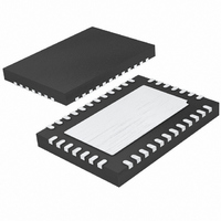
LTC3735EUHF Linear Technology, LTC3735EUHF Datasheet - Page 14

LTC3735EUHF
Manufacturer Part Number
LTC3735EUHF
Description
IC CTRLR DC/DC 2PH HI EFF 38-QFN
Manufacturer
Linear Technology
Datasheet
1.LTC3735EG.pdf
(32 pages)
Specifications of LTC3735EUHF
Applications
Controller, Intel Mobile CPU
Number Of Outputs
1
Voltage - Output
0.7 ~ 1.71 V
Operating Temperature
-40°C ~ 85°C
Mounting Type
Surface Mount
Package / Case
38-QFN
Lead Free Status / RoHS Status
Contains lead / RoHS non-compliant
Voltage - Input
-
Available stocks
Company
Part Number
Manufacturer
Quantity
Price
Company:
Part Number:
LTC3735EUHF
Manufacturer:
LT
Quantity:
10 000
Part Number:
LTC3735EUHF#PBF
Manufacturer:
LINEAR/凌特
Quantity:
20 000
APPLICATIO S I FOR ATIO
LTC3735
Selection criteria for the power MOSFETs include the “ON”
resistance R
pacitance C
continuous drain current I
When the LTC3735 is operating at continuous mode in a
step-down configuration, the duty cycles for the top and
bottom MOSFETs of each power stage are approximately:
The conduction losses of the top and bottom MOSFETs are
therefore:
where I
difference between MOSFET operating temperature and
room temperature, and δ is the temperature dependency
of R
voltage MOSFETs.
The power losses of driving the top and bottom MOSFETs
are simply:
Use Q
switching frequency as described previously. Please no-
tice that the above gate driving losses are usually not
dissipated by the MOSFETs. Instead they are mainly
dissipated on the internal drivers of the LTC3735, if there
are no resistors connected between the drive pins (TG,
BG) and the gates of the MOSFETs.
14
P
P
P
P
Bottom MOSFET Duty Cycle =
Top MOSFET Duty Cycle =
CONTOP
CONBOT
DRTOP
DRBOT
DS(ON)
G
OUT
data at V
= Q
= Q
. δ is roughly 0.004/°C ~ 0.006/°C for low
is the total output current at full load, ΔT is the
RSS
=
=
DS(ON)
•
G
G
V
V
, breakdown voltage BV
V
R
IN
OUT
• PV
• PV
GS
IN
DS ON
–
V
, gate charge Q
= PV
U
(
IN
V
•
CC
CC
OUT
⎛
⎜
⎝
)
I
• f
• f
CC
OUT
2
U
•
D(MAX)
in MOSFET data sheets. f is the
⎛
⎜
⎝
⎞
⎟
⎠
I
2
OUT
2
•
(
.
1
⎞
⎟
⎠
V
G
+
V
2
OUT
W
, reverse transfer ca-
IN
δ
•
V
(
DSS
IN
•
1
Δ
+
–
V
T R
δ
IN
and maximum
V
)
•
OUT
•
Δ
U
DS ON
T
)
(
)
( )
( )
( )
(5)
(6)
( )
4
3
2
1
The calculation of MOSFET switching loss is complicated
by several factors including the wide distribution of power
MOSFET threshold voltage, the nonlinearity of current
rising/falling characteristic and the Miller Effect. Given the
data in a typical power MOSFET data sheet, the switching
losses of the top and bottom MOSFETs can only be
estimated as follows:
where R
mately 2Ω), V
V
MOSFET. Please notice that the switching loss of the
bottom MOSFET is effectively negligible because the cur-
rent conduction of the antiparalleling diode. This effect is
often referred as zero-voltage-transition (ZVT). Similarly
when the LTC3735 converter works under fully synchro-
nous mode at light load, the reverse inductor current can
also go through the body diode of the top MOSFET and
make the turn-on loss to be negligible. However, equa-
tions 7 and 8 have to be used in calculating the worst-case
power loss, which happens at highest load level.
The selection criteria of power MOSFETs start with the
stress check:
and
TH(MIN)
per Phase
P
V
I
P
dissipation specification
P
dissipation specification
MAX
SWBOT
IN
CONTOP
CONBOT
P
< BV
SWTOP
< I
DR
is the minimum gate threshold voltage of the
D(MAX)
≈ 0
DSS
+ P
is the effective driver resistance (of approxi-
+ P
=
SWBOT
DR
⎛
⎜
⎝
SWTOP
V
IN
V
DR
is the driving voltage (= PV
2
4
•
< bottom MOSFET maximum power
–
I
OUT
< top MOSFET maximum power
V
1
TH MIN
• •
(
f C
)
RSS
+
V
TH MIN
•
R
(
1
DR
)
•
⎞
⎟
⎠
CC
) and
3735f
(7)
(8)


