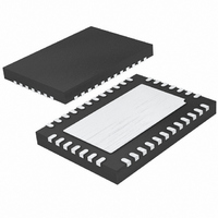
LTC3735EUHF Linear Technology, LTC3735EUHF Datasheet - Page 26

LTC3735EUHF
Manufacturer Part Number
LTC3735EUHF
Description
IC CTRLR DC/DC 2PH HI EFF 38-QFN
Manufacturer
Linear Technology
Datasheet
1.LTC3735EG.pdf
(32 pages)
Specifications of LTC3735EUHF
Applications
Controller, Intel Mobile CPU
Number Of Outputs
1
Voltage - Output
0.7 ~ 1.71 V
Operating Temperature
-40°C ~ 85°C
Mounting Type
Surface Mount
Package / Case
38-QFN
Lead Free Status / RoHS Status
Contains lead / RoHS non-compliant
Voltage - Input
-
Available stocks
Company
Part Number
Manufacturer
Quantity
Price
Company:
Part Number:
LTC3735EUHF
Manufacturer:
LT
Quantity:
10 000
Part Number:
LTC3735EUHF#PBF
Manufacturer:
LINEAR/凌特
Quantity:
20 000
LTC3735
APPLICATIO S I FOR ATIO
PC Board Layout Checklist
When laying out the printed circuit board, the following
checklist should be used to ensure proper operation of the
LTC3735. Check the following in your layout:
1) Are the signal and power grounds segregated? Keep the
SGND at one end of a PC board to prevent MOSFET
currents from traveling under the IC. The IC signal ground
pin should be used to hook up all control circuitry on one
side of the IC, routing the copper through SGND, under the
IC covering the “shadow” of the package, connecting to
the PGND pin and then continuing on to the (–) plate of
C
2) Is the PV
ately adjacent to the PV
capacitor of the X7R or X5R material is small enough to fit
very close to the IC to minimize the ill effects of the large
current pulses drawn to drive the power MOSFETs.
An additional 4.7μF ~ 10μF of ceramic, tantalum or other
low ESR capacitor is recommended in order to keep PV
stable. The power ground returns to the sources of the
bottom N-channel MOSFETs, anodes of the Schottky
diodes, and (–) plates of C
shortest trace length possible.
3) Are the SENSE
minimum PC trace spacing? The filter capacitors between
SENSE
possible to the LTC3735. Ensure accurate current sensing
with Kelvin connections at the current sense resistor. See
Figure 11.
4) Does the (+) plate of C
topside MOSFETs as closely as possible? This capacitor
26
OUT
.
+
and SENSE
CC
decoupling capacitor connected immedi-
–
and SENSE
U
–
CC
pin pairs should be as close as
and PGND pins? A 1μF ceramic
IN
U
connect to the drains of the
IN
+
, which should have the
leads routed together with
TRACE TO INDUCTOR
W
Figure 11. Proper Current Sense Connections
U
PADS OF SENSE RESISTOR
SENSE
CC
+
SENSE
provides the AC current to the MOSFETs. Keep the input
current path formed by the input capacitor, top and bottom
MOSFETs, and the Schottky diode on the same side of the
PC board in a tight loop to minimize conducted and
radiated EMI.
5) Keep the “noisy” nodes, SW, BOOST, TG and BG away
from sensitive small-signal nodes. Ideally the switch
nodes should be placed at the furthest point from the
LTC3735.
The diagram in Figure 12 illustrates all branch currents in
a 2-phase switching regulator. It becomes very clear after
studying the current waveforms why it is critical to keep
the high-switching-current paths to a small physical size.
High electric and magnetic fields will radiate from these
“loops” just as radio stations transmit signals. The output
capacitor ground should return to the negative terminal of
the input capacitor and not share a common ground path
with any switched current paths. The left half of the circuit
gives rise to the “noise” generated by a switching regula-
tor. The ground terminations of the sychronous MOSFETs
and Schottky diodes should return to the negative plate(s)
of the input capacitor(s) with a short isolated PC trace
since very high switched currents are present. A separate
isolated path from the negative plate(s) of the input
capacitor(s) should be used to tie in the IC power ground
pin (PGND) and the signal ground pin (SGND). This
technique keeps inherent signals generated by high cur-
rent pulses from taking alternate current paths that have
finite impedances during the total period of the switching
regulator. External OPTI-LOOP compensation allows over-
compensation for PC layouts which are not optimized but
this is not the recommended design procedure.
–
TRACE TO OUTPUT CAP (+)
3735 F11
3735f


