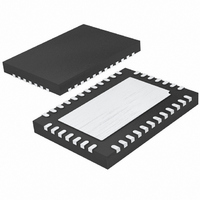
LTC3735EUHF Linear Technology, LTC3735EUHF Datasheet - Page 28

LTC3735EUHF
Manufacturer Part Number
LTC3735EUHF
Description
IC CTRLR DC/DC 2PH HI EFF 38-QFN
Manufacturer
Linear Technology
Datasheet
1.LTC3735EG.pdf
(32 pages)
Specifications of LTC3735EUHF
Applications
Controller, Intel Mobile CPU
Number Of Outputs
1
Voltage - Output
0.7 ~ 1.71 V
Operating Temperature
-40°C ~ 85°C
Mounting Type
Surface Mount
Package / Case
38-QFN
Lead Free Status / RoHS Status
Contains lead / RoHS non-compliant
Voltage - Input
-
Available stocks
Company
Part Number
Manufacturer
Quantity
Price
Company:
Part Number:
LTC3735EUHF
Manufacturer:
LT
Quantity:
10 000
Part Number:
LTC3735EUHF#PBF
Manufacturer:
LINEAR/凌特
Quantity:
20 000
LTC3735
APPLICATIO S I FOR ATIO
The worst-case RMS ripple current for a single stage
design peaks at an input voltage of twice the output
voltage. The worst-case RMS ripple current for a two
stage design results in peak outputs of 1/4 and 3/4 of input
voltage. When the RMS current is calculated, higher
effective duty factor results and the peak current levels are
divided as long as the currents in each stage are balanced.
Refer to Linear Technology Application Note 19 for a
detailed description of how to calculate RMS current for
the single stage switching regulator. Figures 3 and 4
illustrate how the input and output currents are reduced
by using an additional phase. The input current peaks
drop in half and the frequency is doubled for this 2-phase
converter. The input capacity requirement is thus reduced
theoretically by a factor of four! Ceramic input capacitors
with their low ESR characteristics can be used.
Figure 4 illustrates the RMS input current drawn from the
input capacitance vs the duty cycle as determined by the
ratio of input and output voltage. The peak input RMS
current level of the single phase system is reduced by 50%
in a 2-phase solution due to the current splitting between
the two stages.
28
U
U
W
U
An interesting result of the 2-phase solution is that the V
which produces worst-case ripple current for the input
capacitor, V
duces zero input current ripple in the 2-phase design.
The output ripple current is reduced significantly when
compared to the single phase solution using the same
inductance value because the V
term from the stage that has its bottom MOSFET on
subtracts current from the (V
resulting from the stage which has its top MOSFET on. The
output ripple current is:
where D is duty factor.
The input and output ripple frequency is increased by the
number of stages used, reducing the output capacity
requirements. When V
as illustrated in Figures 3 and 4, very low input and output
ripple currents result.
Δ
I
RIPPLE
OUT
=
2
= V
V
fL
OUT
IN
/2, in the single phase design pro-
⎡
⎢
⎢
⎣
IN
1 2 1
is approximately equal to 2(V
–
1 2
–
D
IN
D
( – )
– V
+
OUT
OUT
1
D
/L discharge current
⎤
⎥
⎥
⎦
)/L charging current
OUT
3735f
IN
)


