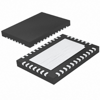
LTC3735EUHF Linear Technology, LTC3735EUHF Datasheet - Page 23

LTC3735EUHF
Manufacturer Part Number
LTC3735EUHF
Description
IC CTRLR DC/DC 2PH HI EFF 38-QFN
Manufacturer
Linear Technology
Datasheet
1.LTC3735EG.pdf
(32 pages)
Specifications of LTC3735EUHF
Applications
Controller, Intel Mobile CPU
Number Of Outputs
1
Voltage - Output
0.7 ~ 1.71 V
Operating Temperature
-40°C ~ 85°C
Mounting Type
Surface Mount
Package / Case
38-QFN
Lead Free Status / RoHS Status
Contains lead / RoHS non-compliant
Voltage - Input
-
Available stocks
Company
Part Number
Manufacturer
Quantity
Price
Company:
Part Number:
LTC3735EUHF
Manufacturer:
LT
Quantity:
10 000
Part Number:
LTC3735EUHF#PBF
Manufacturer:
LINEAR/凌特
Quantity:
20 000
APPLICATIO S I FOR ATIO
topside MOSFET and the synchronous MOSFET. If the two
MOSFETs have approximately the same R
resistance of one MOSFET can simply be summed with the
resistances of L, R
example, if each R
= 5mΩ, then the total resistance is 25mΩ. This results in
losses ranging from 2% to 8% as the output current
increases from 3A to 15A per output stage for a 5V output,
or a 3% to 12% loss per output stage for a 3.3V output.
Efficiency varies as the inverse square of V
same external components and output power level. The
combined effects of increasingly lower output voltages
and higher currents required by high performance digital
systems is not doubling but quadrupling the importance of
loss terms in the switching regulator system!
2) Transition losses apply only to the topside MOSFET(s),
and are significant only when operating at high input
voltages (typically 12V or greater). Transition losses can
be estimated from:
3) PV
driver current results from switching the gate capacitance
of the power MOSFETs. Each time a MOSFET gate is
switched from low to high to low again, a packet of charge
dQ moves from PV
current out of PV
control circuit current. In continuous mode, I
(Q
topside and bottom side MOSFETs and f is the switching
frequency.
4) The input capacitor has the difficult job of filtering the
large RMS input current to the regulator. It must have a
very low ESR to minimize the AC I
capacitance to prevent the RMS current from causing
T
Transition Loss =
+ Q
CC
B
drives both top and bottom MOSFETs. The MOSFET
per Phase
)f, where Q
CC
DS(ON)
SENSE
CC
U
that is typically much larger than the
T
⎛
⎜
⎝
V
and Q
to ground. The resulting dQ/dt is a
IN
V
DR
and ESR to obtain I
= 10mΩ, R
2
U
4
•
–
I
B
OUT
V
are the gate charges of the
1
TH MIN
• •
(
f C
2
L
W
R loss and sufficient
= 10mΩ, and R
)
RSS
+
V
DS(ON)
TH MIN
•
2
R losses. For
R
(
1
OUT
DR
GATECHG
U
, then the
)
•
⎞
⎟
⎠
for the
SENSE
=
additional upstream losses in fuses or batteries. The
LTC3735 2-phase architecture typically halves the input
and output capacitor requirements over 1-phase
solutions.
Other losses, including C
conduction loss during dead time, inductor core loss and
internal control circuitry supply current generally account
for less than 2% additional loss.
Checking Transient Response
The regulator loop response can be checked by looking at
the load transient response. Switching regulators take
several cycles to respond to a step in DC (resistive) load
current. When a load step occurs, V
amount equal to ΔI
series resistance of C
discharge C
forces the regulator to adapt to the current change and
return V
time V
ringing, which would indicate a stability problem. The
availability of the I
control loop behavior but also provides a DC coupled and
AC filtered closed loop response test point. The DC step,
rise time, and settling at this test point truly reflects the
closed loop response. Assuming a predominantly second
order system, phase margin and/or damping factor can be
estimated using the percentage of overshoot seen at this
pin. The bandwidth can also be estimated by examining
the rise time at the pin. The I
shown in the Figure 1 circuit will provide an adequate
starting point for most applications.
The I
loop compensation. The values can be modified slightly
(from 0.2 to 5 times their suggested values) to optimize
transient response once the final PC layout is done and the
particular output capacitor type and value have been
determined. The output capacitors need to be decided
upon first because the various types and values determine
TH
OUT
OUT
series R
can be monitored for excessive overshoot or
OUT
to its steady-state value. During this recovery
generating the feedback error signal that
C
-C
TH
LOAD
C
OUT
pin not only allows optimization of
filter sets the dominant pole-zero
(ESR), where ESR is the effective
. ΔI
OUT
LOAD
ESR loss, Schottky diode
TH
also begins to charge or
external components
OUT
LTC3735
shifts by an
23
3735f


