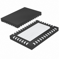
LTC3735EUHF Linear Technology, LTC3735EUHF Datasheet - Page 15

LTC3735EUHF
Manufacturer Part Number
LTC3735EUHF
Description
IC CTRLR DC/DC 2PH HI EFF 38-QFN
Manufacturer
Linear Technology
Datasheet
1.LTC3735EG.pdf
(32 pages)
Specifications of LTC3735EUHF
Applications
Controller, Intel Mobile CPU
Number Of Outputs
1
Voltage - Output
0.7 ~ 1.71 V
Operating Temperature
-40°C ~ 85°C
Mounting Type
Surface Mount
Package / Case
38-QFN
Lead Free Status / RoHS Status
Contains lead / RoHS non-compliant
Voltage - Input
-
Available stocks
Company
Part Number
Manufacturer
Quantity
Price
Company:
Part Number:
LTC3735EUHF
Manufacturer:
LT
Quantity:
10 000
Part Number:
LTC3735EUHF#PBF
Manufacturer:
LINEAR/凌特
Quantity:
20 000
APPLICATIO S I FOR ATIO
The maximum power dissipation allowed for each MOSFET
depends heavily on MOSFET manufacturing and packag-
ing, PCB layout and power supply cooling method.
Maximum power dissipation data are usually specified in
MOSFET data sheets under different PCB mounting
conditions.
The next step of selecting power MOSFETs is to minimize
the overall power loss:
For typical mobile CPU applications where the ratio be-
tween input and output voltages is higher than 2:1, the
bottom MOSFET conducts load current most of the time
while the main losses of the top MOSFET are for switching
and driving. Therefore a low R
in parallel) would minimize the conduction loss of the
bottom MOSFET while a higher R
C
The Schottky diodes, D1 and D2 in Figure 1 conduct during
the dead-time between the conduction of the top and
bottom MOSFETs. This helps reduce the current flowing
through the body diode of the bottom MOSFET. A body
diode usually has a forward conduction voltage higher
than that of a Schottky and is thus detrimental to effi-
ciency. The charge storage and reverse recovery of a body
diode also cause high frequency rings at the switching
nodes (the conjunction nodes between the top and bottom
MOSFETs), which are again not desired for efficiency or
EMI. Some power MOSFET manufacturers integrate a
Schottky diode with a power MOSFET, eliminating the
need to parallel an external Schottky. These integrated
Schottky-MOSFETs, however, have smaller MOSFET die
sizes than conventional parts and are thus not suitable for
high current applications.
C
In continuous mode, the source current of each top
N-channel MOSFET is a square wave of duty cycle V
V
RSS
IN
IN
P
. A low ESR input capacitor sized for the maximum
and C
OVL
part would be desirable for the top MOSFET.
= P
= (P
OUT
P
TOP
DRBOT
CONTOP
Selection
+ P
+ P
BOT
U
+ P
SWBOT
DRTOP
U
)
DS(ON)
+ P
DS(ON)
SWTOP
W
part (or multiple parts
but lower Q
) + (P
CONBOT
U
G
OUT
and
+
/
RMS current must be used. The details of a closed form
equation can be found in Linear Technology Application
Note 77. Figure 4 shows the input capacitor ripple current
for a 2-phase configuration with the output voltage fixed
and input voltage varied. The input ripple current is nor-
malized against the DC output current. The graph can be
used in place of tedious calculations. The minimum input
ripple current can be achieved when the input voltage is
twice the output voltage.
In the graph of Figure 4, the 2-phase local maximum input
RMS capacitor currents are reached when:
These worst-case conditions are commonly used for
design, considering input/output variations and long
term reliability. Note that capacitor manufacturer’s ripple
current ratings are often based on only 2000 hours of life.
This makes it advisable to further derate the capacitor, or
to choose a capacitor rated at a higher temperature than
required. Several capacitors may also be paralleled to
meet size or height requirements in the design. Always
consult the capacitor manufacturer if there is any
question.
where k = 1, 2
V
V
OUT
IN
Figure 4. Normalized RMS Input Ripple Current
vs Duty Factor for 1 and 2 Output Stages
=
0.6
0.5
0.4
0.3
0.2
0.1
2
0
0.1
k
4
−
0.2
1
1-PHASE
2-PHASE
0.3
DUTY FACTOR (V
0.4
0.5
OUT
0.6
/V
IN
0.7
)
0.8
3735 F04
LTC3735
0.9
15
3735f


