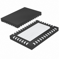
LTC3735EUHF Linear Technology, LTC3735EUHF Datasheet - Page 19

LTC3735EUHF
Manufacturer Part Number
LTC3735EUHF
Description
IC CTRLR DC/DC 2PH HI EFF 38-QFN
Manufacturer
Linear Technology
Datasheet
1.LTC3735EG.pdf
(32 pages)
Specifications of LTC3735EUHF
Applications
Controller, Intel Mobile CPU
Number Of Outputs
1
Voltage - Output
0.7 ~ 1.71 V
Operating Temperature
-40°C ~ 85°C
Mounting Type
Surface Mount
Package / Case
38-QFN
Lead Free Status / RoHS Status
Contains lead / RoHS non-compliant
Voltage - Input
-
Available stocks
Company
Part Number
Manufacturer
Quantity
Price
Company:
Part Number:
LTC3735EUHF
Manufacturer:
LT
Quantity:
10 000
Part Number:
LTC3735EUHF#PBF
Manufacturer:
LINEAR/凌特
Quantity:
20 000
APPLICATIO S I FOR ATIO
Start-Up Sequence (Refer to the Functional Diagram)
After soft-start, the output voltage of the regulator settles
at a voltage level equal to V
By using different R5 resistors, V
An internal 1.5μA current source charges up the soft-start
capacitor, C
1.5V, the controller is permitted to start operating. As the
voltage on RUN/SS increases from 1.5V to 3.0V, the
internal current limit is increased from 25mV/R
72mV/R
eliminating the starting surge current required from the
input power supply. If RUN/SS has been pulled all the way
to ground there is a delay before starting of approximately:
The time for the output current to ramp up is then:
By pulling the RUN/SS pin below 1V the LTC3735 is put
into low current shutdown (I
can be driven directly from logic as shown in Figure 6.
Diode D1 in Figure 6 reduces the start delay but allows
C
The RUN/SS pin has an internal 6V zener clamp (see
Functional Diagram).
SS
V
t
t
DELAY
IRAMP
BOOT
to ramp up slowly providing the soft-start function.
3.3V OR 5V
*OPTIONAL TO DEFEAT OVERCURRENT LATCHOFF
SENSE
=
=
=
0 6
SS
1 5
3
.
1 5
. The output current thus ramps up slowly,
Figure 6. RUN/SS Pin Interfacing
.
V
D1
. When the voltage on RUN/SS reaches
.
1 5
V
μ
.
−
V
PV
•
A
1 5
μ
R
CC
R
U
.
C
A
R
2
5
SS
SS
V
•
•
*
RUN/SS
C
(
(
=
R
R
SS
U
3
1
(
1
BOOT
+
C
+
s F C
=
Q
SS
/
R
R
< 100μA). The RUN/SS pin
μ
(
1
2
5
BOOT
.
s F C
)
)
)
/
μ
W
SS
can be programmed.
)
SS
RUN/SS
U
3735 F06
SENSE
C
SS
to
(=(INTERNAL PG)
After the output voltage enters the ±10% regulation win-
dow centered at V
tor issues a logic high signal. Refer to the timing diagram
in Figure 7. This signal then enters a logic AND gate, with
MCH_PG being the other input, and the output of the gate
is PG shown in Figure 7. This composite PG signal is then
delayed by t
As soon as MD is asserted, the output voltage changes
from V
six VID bits. In the LTC3735, the time t
switching cycles:
If f
If f
AND (MCH_PG))
COMPOSITE PG
COMPARATOR)
POWER GOOD
INTERNAL PG
S
S
t
(OUTPUT OF
BOOT
is set at 210kHz, t
is set at 550kHz, t
INTERNAL
MCH_PG
VID BITS
RUN/SS
BOOT
V
OUT
MD
= 15
to V
BOOT
Figure 7. Start-Up Timing Diagram
f
1
VID
S
BOOT
amount of time and then becomes MD.
, a voltage level totally controlled by the
INVALID
1.5V
, the internal power good compara-
BOOT
BOOT
V
BOOT
90% V
= 71μs
= 27μs
BOOT
t
TIME
BOOT
BOOT
LTC3735
V
VALID
is set to be 15
VID
19
3735 F07
3735f


