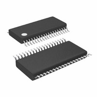
LTC3829EFE#PBF Linear Technology, LTC3829EFE#PBF Datasheet - Page 12

LTC3829EFE#PBF
Manufacturer Part Number
LTC3829EFE#PBF
Description
IC BUCK SYNC ADJ 38TSSOP
Manufacturer
Linear Technology
Type
Step-Down (Buck)r
Datasheet
1.LTC3829EFEPBF.pdf
(40 pages)
Specifications of LTC3829EFE#PBF
Internal Switch(s)
No
Synchronous Rectifier
Yes
Number Of Outputs
1
Voltage - Output
0.6 ~ 5 V
Frequency - Switching
250kHz ~ 770kHz
Voltage - Input
4.5 ~ 38 V
Operating Temperature
-40°C ~ 125°C
Mounting Type
Surface Mount
Package / Case
38-TSSOP Exposed Pad, 38-eTSSOP, 38-HTSSOP
Lead Free Status / RoHS Status
Lead free / RoHS Compliant
Current - Output
-
Power - Output
-
Available stocks
Company
Part Number
Manufacturer
Quantity
Price
operaTion
LTC3829
Main Control Loop
The LTC3829 uses a constant frequency, current mode
step-down architecture. During normal operation, each
top MOSFET is turned on each cycle when the oscillator
sets the RS latch, and turned off when the main current
comparator, I
current at which I
the voltage on the I
ror amplifier, EA. The remote sense amplifier (DIFFAMP)
produces a signal equal to the differential voltage sensed
across the output capacitor and re-references it to the lo-
cal IC ground reference. The V
this feedback signal and compares it to the internal 0.6V
reference. When the load current increases, it causes a
slight decrease in the V
reference, which in turn causes the I
until each inductor’s average current equals one-third of
the new load current (assuming all three current sensing
resistors are equal). After each top MOSFET has turned off,
the bottom MOSFET is turned on until either the inductor
current starts to reverse, as indicated by the reverse current
comparator, I
The main control loop is shut down by pulling the RUN pin
low. Releasing RUN allows an internal 1.0µA current source
to pull up the RUN pin. When the RUN pin reaches 1.22V,
the main control loop is enabled and the IC is powered
up. When the RUN pin is low, all functions are kept in a
controlled state.
INTV
Power for the top and bottom MOSFET drivers and most
other internal circuitry is derived from the INTV
When the EXTV
than 4.7V, an internal 5V linear regulator supplies INTV
power from V
regulator is turned off and an internal switch is turned on
connecting EXTV
power to be derived from a high efficiency external source
such as a switching regulator output. Each top MOSFET
driver is biased from the floating bootstrap capacitor, C
CC
/EXTV
CMP
CC
REV
IN
CC
Power
. If EXTV
CC
, or the beginning of the next cycle.
, resets each RS latch. The peak inductor
CMP
pin is left open or tied to a voltage less
. Using the EXTV
TH
(Refer to Functional Diagram)
resets the RS latch is controlled by
pin, which is the output of the er-
FB
CC
pin voltage relative to the 0.6V
is taken above 4.7V, the 5V
FB
pin receives a portion of
CC
TH
pin allows the INTV
voltage to increase
CC
pin.
CC
CC
B
,
which normally recharges during each off cycle through
an external diode when the top MOSFET turns off. If the
input voltage, V
the loop may enter dropout and attempt to turn on the
top MOSFET continuously. The dropout detector detects
this and forces the top MOSFET off for about one-twelfth
of the clock period plus 100ns every third cycle to allow
C
be present or the IC operates at low frequency during the
dropout transition to ensure C
Shutdown and Start-Up (RUN and TK/SS Pins)
The LTC3829 can be shut down using the RUN pin. Pulling
the RUN pin below 1.22V shuts down the main control loop
for the controller and most internal circuits, including the
INTV
1.0µA current to pull up the pin and enable the controller.
Alternatively, the RUN pin may be externally pulled up or
driven directly by logic. Be careful not to exceed the ab-
solute maximum rating of 6V on this pin. The start-up of
the controller’s output voltage, V
voltage on the TK/SS pin. When the voltage on the TK/SS
pin is less than the 0.6V internal reference, the LTC3829
regulates the V
of the 0.6V reference. This allows the TK/SS pin to be
used to program a soft-start by connecting an external
capacitor from the TK/SS pin to SGND. An internal 1.25µA
pull-up current charges this capacitor, creating a voltage
ramp on the TK/SS pin. As the TK/SS voltage rises linearly
from 0V to 0.6V (and beyond), the output voltage, V
rises smoothly from zero to its final value. Alternatively,
the TK/SS pin can be used to cause the start-up of V
to track that of another supply. Typically, this requires
connecting to the TK/SS pin an external resistor divider
from the other supply to ground (see the Applications
Information section). When the RUN pin is pulled low to
disable the controller, or when INTV
undervoltage lockout threshold of 3.3V, the TK/SS pin is
pulled low by an internal MOSFET. When in undervoltage
lockout, all phases of the controller are disabled and the
external MOSFETs are held off.
B
to recharge. However, it is recommended that a load
CC
regulator. Releasing the RUN pin allows an internal
FB
IN
voltage to the TK/SS pin voltage instead
, decreases to a voltage close to V
B
is recharged.
OUT
, is controlled by the
CC
drops below its
OUT
OUT
OUT
3829f
,
,


